© 2000 IXYS All rights reserved
98739 (8/00)
Symbol
Test Conditions
Maximum Ratings
V
DSS
T
J
= 25
∞
C to 150
∞
C
100
V
V
DGR
T
J
= 25
∞
C to 150
∞
C; R
GS
= 1 M
100
V
V
GS
Continuous
±
20
V
V
GSM
Transient
±
30
V
I
D25
T
C
= 25
∞
C
80
A
I
L(RMS)
Lead current limit
75
A
I
DM
T
C
= 25
∞
C, pulse width limited by T
JM
320
A
I
AR
T
C
= 25
∞
C
80
A
E
AR
T
C
= 25
∞
C
50
mJ
E
AS
2.5
J
dv/dt
I
S
I
DM
, di/dt
100 A/
µ
s, V
DD
V
DSS
,
5
V/ns
T
J
150
∞
C, R
G
= 2
P
D
T
C
= 25
∞
C
300
W
T
J
-55 to +150
∞
C
T
JM
150
∞
C
T
stg
-55 to +150
∞
C
T
L
1.6 mm (0.063 in) from case for 10 s 300
∞
C
M
d
Mounting torque
1.13/10 Nm/lb.in.
Weight
TO-247 6
g
TO-268 4
g
N-Channel Enhancement Mode
Avalanche Rated, High dv/dt
Preliminary data sheet
Features
l
International standard packages
l
Low R
DS (on)
l
Rated for unclamped Inductive load
switching (UIS)
l
Molding epoxies meet UL
94
V-0
flammability classification
Advantages
l
Easy to mount
l
Space savings
l
High power density
Symbol
Test Conditions
Characteristic Values
(T
J
= 25
∞
C, unless otherwise specified)
min.
typ.
max.
V
DSS
V
GS
= 0 V, I
D
= 1 mA
100
V
V
GS(th)
V
DS
= V
GS
, I
D
= 4 mA
2.0
4.0
V
I
GSS
V
GS
=
±
20 V
DC
, V
DS
= 0
±
100
nA
I
DSS
V
DS
= V
DSS
T
J
= 25
∞
C
50
µ
A
V
GS
= 0 V
T
J
= 125
∞
C
1
mA
R
DS(on)
V
GS
= 10 V, I
D
= 0.5 I
D25
12.5 m
Pulse test, t
300
µ
s, duty cycle d
2 %
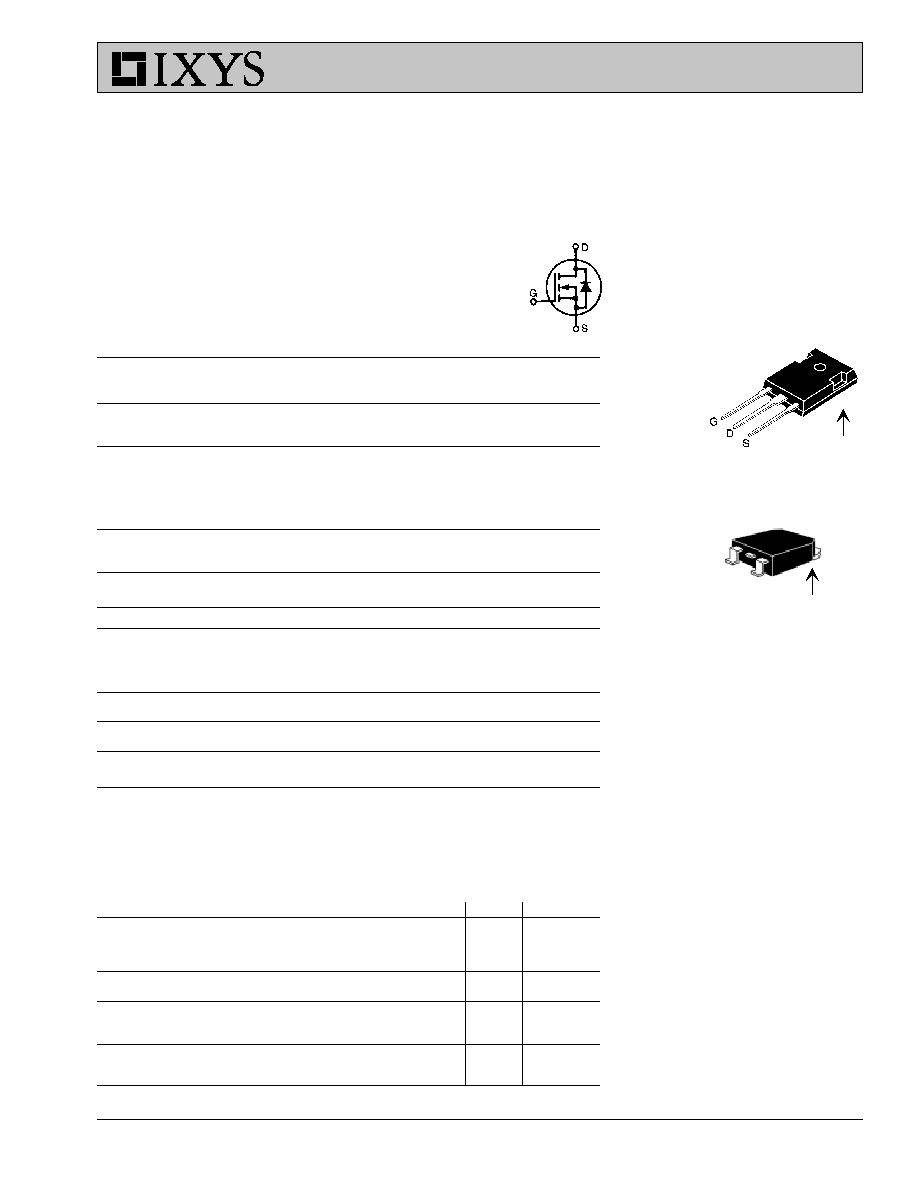
TO-247 AD (IXFH)
G = Gate D = Drain
S = Source TAB = Drain
HiPerFET
TM
Power MOSFETs
TO-268 ( IXFT) Case Style
(TAB)
G
S
V
DSS
= 100 V
I
D25
= 80 A
R
DS(on)
= 12.5 m
t
rr
200 ns
IXFH 80N10
IXFT 80N10
(TAB)
IXYS MOSFETS and IGBTs are covered by one or more of the following U.S. patents:
4,835,592
4,881,106
5,017,508
5,049,961
5,187,117
5,486,715
4,850,072
4,931,844
5,034,796
5,063,307
5,237,481
5,381,025
IXYS reserves the right to change limits, test conditions, and dimensions.
IXFH 80N10
IXFT 80N10
Symbol
Test Conditions
Characteristic Values
(T
J
= 25
∞
C, unless otherwise specified)
min.
typ.
max.
g
fs
V
DS
= 10 V; I
D
= 0.5 ∑ I
D25
, pulse test
35
55
S
C
iss
4800
pF
C
oss
V
GS
= 0 V, V
DS
= 25 V, f = 1 MHz
1460
pF
C
rss
490
pF
t
d(on)
41
ns
t
r
V
GS
= 10 V, V
DS
= 0.5 ∑ V
DSS
, I
D
= 0.5 ∑ I
D25
63
ns
t
d(off)
R
G
= 2.5
(External),
90
ns
t
f
26
ns
Q
g(on)
180
nC
Q
gs
V
GS
= 10 V, V
DS
= 0.5 ∑ V
DSS
, I
D
= 0.5 ∑ I
D25
38
nC
Q
gd
65
nC
R
thJC
0.42
K/W
R
thCK
(TO-247)
0.25
K/W
Source-Drain Diode
Characteristic Values
(T
J
= 25
∞
C, unless otherwise specified)
Symbol
Test Conditions
min.
typ.
max.
I
S
V
GS
= 0 V
80
A
I
SM
Repetitive; pulse width limited by T
JM
320
A
V
SD
I
F
= I
S
, V
GS
= 0 V,
1.5
V
Pulse test, t
300
µ
s, duty cycle d
2 %
t
rr
200
ns
Q
RM
I
F
= 25A, -di/dt = 100 A/
µ
s, V
R
= 50 V
0.5
µ
C
I
RM
6
A
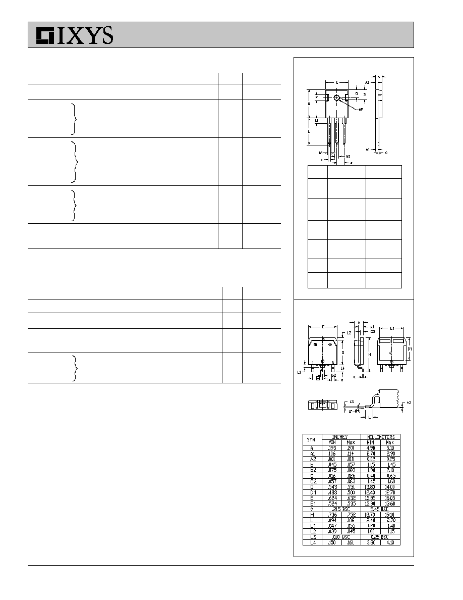
TO-268 Outline
Dim.
Millimeter
Inches
Min.
Max.
Min.
Max.
A
4.7
5.3
.185
.209
A
1
2.2
2.54
.087
.102
A
2
2.2
2.6
.059
.098
b
1.0
1.4
.040
.055
b
1
1.65
2.13
.065
.084
b
2
2.87
3.12
.113
.123
C
.4
.8
.016
.031
D
20.80
21.46
.819
.845
E
15.75
16.26
.610
.640
e
5.20
5.72
0.205
0.225
L
19.81
20.32
.780
.800
L1
4.50
.177
P3.55
3.65
.140
.144
Q
5.89
6.40
0.232
0.252
R
4.32
5.49
.170
.216
S
6.15
BSC
242
BSC
Terminals:
1 - Gate
2 - Drain
3 - Source
Tab - Drain
1 2 3
TO-247 AD (IXFH) Outline
Terminals: 1 - Gate
2 - Drain
3 - Source
Tab - Drain