1 - 4
© 2000 IXYS All rights reserved
Symbol
Test Conditions
Maximum Ratings
V
DSS
T
J
= 25
∞
C to 150
∞
C
1000
V
V
DGR
T
J
= 25
∞
C to 150
∞
C; R
GS
= 1 M
W
1000
V
V
GS
Continuous
±
20
V
V
GSM
Transient
±
30
V
I
D25
T
C
= 25
∞
C
14N100
14
A
15N100
15
A
I
DM
T
C
= 25
∞
C, pulse width limited by T
JM
14N100
56
A
15N100
60
A
I
AR
T
C
= 25
∞
C
14N100
14
A
15N100
15
A
E
AR
T
C
= 25
∞
C
45
mJ
dv/dt
I
S
£
I
DM
, di/dt
£
100 A/
m
s, V
DD
£
V
DSS
,
5
V/ns
T
J
£
150
∞
C, R
G
= 2
W
P
D
T
C
= 25
∞
C
360
W
T
J
-55 ... +150
∞
C
T
JM
150
∞
C
T
stg
-55 ... +150
∞
C
T
L
1.6 mm (0.062 in.) from case for 10 s
300
∞
C
M
d
Mounting torque
1.13/10 Nm/lb.in.
Weight
6
g
Symbol
Test Conditions
Characteristic Values
(T
J
= 25
∞
C, unless otherwise specified)
min.
typ.
max.
V
DSS
V
GS
= 0 V, I
D
= 1 mA
1000
V
V
GS(th)
V
DS
= V
GS
, I
D
= 4 mA
2.5
4.5
V
I
GSS
V
GS
=
±
20 V
DC
, V
DS
= 0
±
100
nA
I
DSS
V
DS
= 0.8 ∑ V
DSS
T
J
=
25
∞
C
250
m
A
V
GS
= 0 V
T
J
= 125
∞
C
1
mA
R
DS(on)
V
GS
= 10 V, I
D
= 0.5 ∑ I
D25
14N100
0.75
W
15N100
0.70
W
Pulse test, t
£
300
m
s, duty cycle d
£
2 %
N-Channel Enhancement Mode
High dv/dt, Low t
rr
, HDMOS
TM
Family
TO-247 AD
(IXFH)
Features
q
International standard packages
q
Low R
DS (on)
HDMOS
TM
process
q
Rugged polysilicon gate cell structure
q
Unclamped Inductive Switching (UIS)
rated
q
Low package inductance
- easy to drive and to protect
q
Fast intrinsic Rectifier
Applications
q
DC-DC converters
q
Battery chargers
q
Switched-mode and resonant-mode
power supplies
q
DC choppers
q
AC motor control
q
Temperature and lighting controls
Advantages
q
Easy to mount with 1 screw (TO-247)
(isolated mounting screw hole) or
mounting clip or spring (PLUS 247
TM
)
q
High power surface mountable package
q
High power density
V
DSS
I
D25
R
DS(on)
IXFH/IXFT/IXFX14
N100 1000 V
14 A 0.75
W
IXFH/IXFT/IXFX15
N100 1000 V
15 A 0.70
W
t
rr
£
200 ns
(TAB)
HiPerFET
TM
Power MOSFETs
97535B (1/99)
PLUS 247
TM
(IXFX)
G
D
Preliminary data sheet
TO-268 (D3)
(IXFT)
(TAB)
G
S
(TAB)
IXYS reserves the right to change limits, test conditions, and dimensions.
2 - 4
© 2000 IXYS All rights reserved
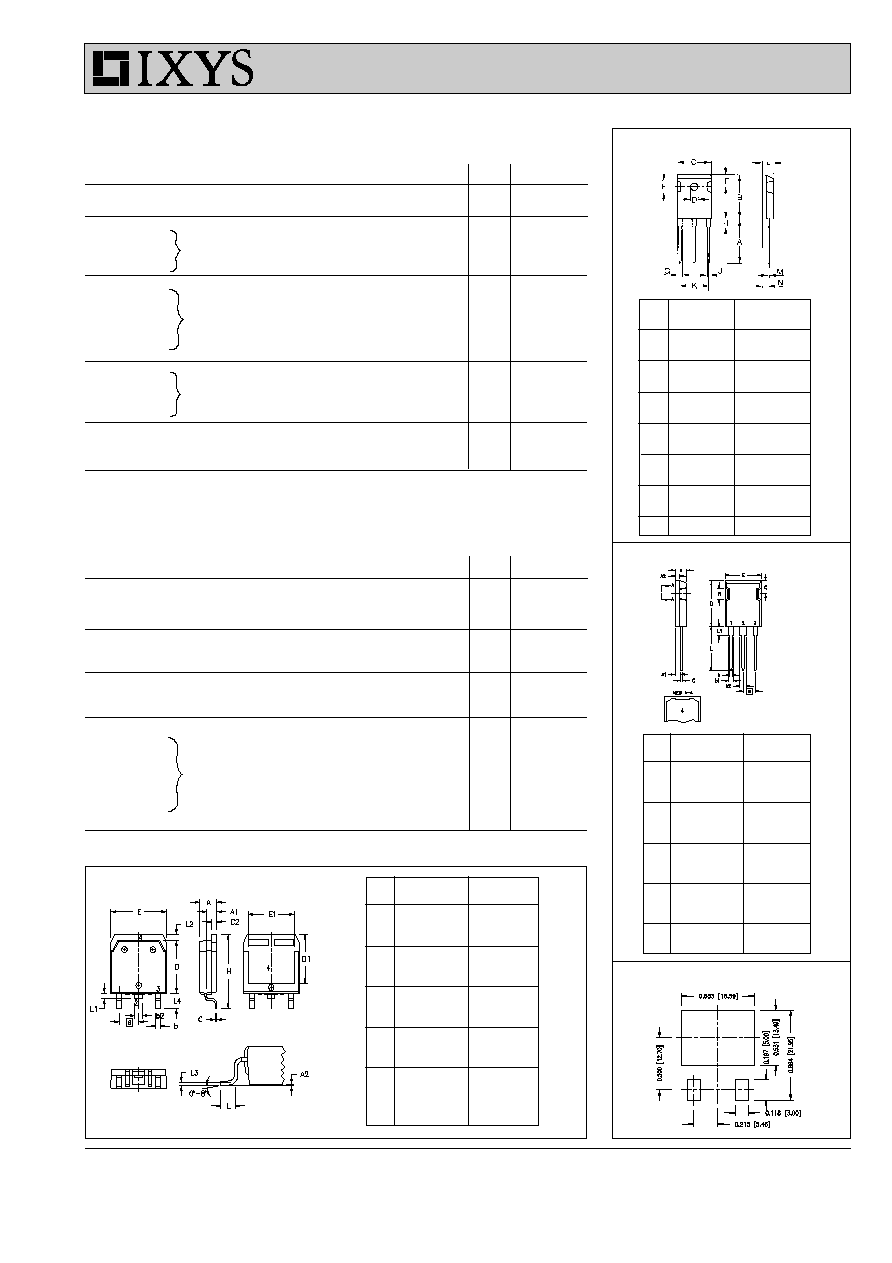
TO-247 AD (IXFH) Outline
Dim. Millimeter
Inches
Min.
Max.
Min.
Max.
A
19.81 20.32
0.780 0.800
B
20.80 21.46
0.819 0.845
C
15.75 16.26
0.610 0.640
D
3.55
3.65
0.140 0.144
E
4.32
5.49
0.170 0.216
F
5.4
6.2
0.212 0.244
G
1.65
2.13
0.065 0.084
H
-
4.5
-
0.177
J
1.0
1.4
0.040 0.055
K
10.8
11.0
0.426 0.433
L
4.7
5.3
0.185 0.209
M
0.4
0.8
0.016 0.031
N
1.5
2.49
0.087 0.102
Dim.
Millimeter
Inches
Min.
Max.
Min.
Max.
A
4.9
5.1
.193
.201
A
1
2.7
2.9
.106
.114
A
2
.02
.25
.001
.010
b
1.15
1.45
.045
.057
b
2
1.9
2.1
.75
.83
C
.4
.65
.016
.026
D
13.80
14.00
.543
.551
E
15.85
16.05
.624
.632
E
1
13.3
13.6
.524
.535
e 5.45 BSC .215 BSC
H
18.70
19.10
.736
.752
L
2.40
2.70
.094
.106
L1
1.20
1.40
.047
.055
L2
1.00
1.15
.039
.045
L3 0.25 BSC .010 BSC
L4
3.80
4.10
.150
.161
TO-268AA (D
3
PAK)
PLUS247
TM
(IXFX) Outline
Dim.
Millimeter
Inches
Min.
Max.
Min. Max.
A
4.83
5.21
.190 .205
A
1
2.29
2.54
.090 .100
A
2
1.91
2.16
.075 .085
b
1.14
1.40
.045 .055
b
1
1.91
2.13
.075 .084
b
2
2.92
3.12
.115 .123
C
0.61
0.80
.024 .031
D
20.80
21.34
.819 .840
E
15.75
16.13
.620 .635
e 5.45 BSC
.215 BSC
L
19.81
20.32
.780 .800
L1
3.81
4.32
.150 .170
Q
5.59
6.20
.220 .244
R
4.32
4.83
.170 .190
Min. Recommended Footprint
Symbol
Test Conditions
Characteristic Values
(T
J
= 25
∞
C, unless otherwise specified)
min.
typ.
max.
g
fs
V
DS
= 10 V; I
D
= 0.5 ∑ I
D25
, pulse test
6
10
S
C
iss
4500
pF
C
oss
V
GS
= 0 V, V
DS
= 25 V, f = 1 MHz
430
pF
C
rss
150
pF
t
d(on)
27
ns
t
r
V
GS
= 10 V, V
DS
= 0.5 ∑ V
DSS
, I
D
= 0.5 ∑ I
D25
30
ns
t
d(off)
R
G
= 2
W
(External),
120
ns
t
f
30
ns
Q
g(on)
220
nC
Q
gs
V
GS
= 10 V, V
DS
= 0.5 ∑ V
DSS
, I
D
= 0.5 ∑ I
D25
30
nC
Q
gd
85
nC
R
thJC
0.35
K/W
R
thCK
0.25
K/W
Source-Drain Diode
Characteristic Values
(T
J
= 25
∞
C, unless otherwise specified)
Symbol
Test Conditions
min.
typ.
max.
I
S
V
GS
= 0 V
14N100
14
A
15N100
15
A
I
SM
Repetitive;
14N100
56
A
pulse width limited by T
JM
15N100
60
A
V
SD
I
F
= I
S
, V
GS
= 0 V,
1.5
V
Pulse test, t
£
300
m
s, duty cycle d
£
2 %
t
rr
T
J
=
25
∞
C
200
ns
T
J
= 125
∞
C
350
ns
Q
RM
T
J
=
25
∞
C
1
m
C
T
J
= 125
∞
C
2
m
C
I
RM
T
J
=
25
∞
C
10
A
T
J
= 125
∞
C
15
A
I
F
= I
S
-di/dt = 100 A/
m
s,
V
R
= 100 V
(TO-247 Case Style)
IXFH14N100
IXFT14N100
IXFX15N100
IXFH15N100
IXFT15N100
IXFX14N100
IXYS MOSFETS and IGBTs are covered by one or more of the following U.S. patents:
4,835,592
4,881,106
5,017,508
5,049,961
5,187,117
5,486,715
4,850,072
4,931,844
5,034,796
5,063,307
5,237,481
5,381,025
3 - 4
© 2000 IXYS All rights reserved
IXFH14N100
IXFT14N100
IXFX15N100
IXFH15N100
IXFT15N100
IXFX14N100
V
GS
- Volts
2.0
2.5
3.0
3.5
4.0
4.5
5.0
I
D
-
A
m
per
e
s
0
2
4
6
8
10
12
14
T
C
- Degrees C
-50 -25
0
25
50
75
100 125 150
I
D
- A
m
p
e
r
e
s
0
4
8
12
16
20
T
J
- Degrees C
25
50
75
100
125
150
R
DS
(
O
N)
-
No
rmal
ized
1.0
1.2
1.4
1.6
1.8
2.0
2.2
I
D
= 7.5A
I
D
- Amperes
0
3
6
9
12
15
R
DS
(
O
N)
- N
o
rmali
z
ed
0.8
1.0
1.2
1.4
1.6
1.8
2.0
V
DS
- Volts
0
4
8
12
16
20
I
D
- A
m
p
e
r
e
s
0
4
8
12
16
V
DS
- Volts
0
4
8
12
16
20
I
D
- A
m
p
e
r
e
s
0
4
8
12
16
20
4V
V
GS
= 10V
V
GS
= 9V
8V
7V
6V
T
J
= 125
O
C
V
GS
= 10V
T
J
= 25
O
C
5V
5V
4V
T
J
= 25
o
C
I
D
= 15A
T
J
= 25
O
C
IXF_15N100
T
J
= 125
o
C
V
GS
= 9V
8V
7V
6V
T
J
= 125
O
C
IXF_14N100
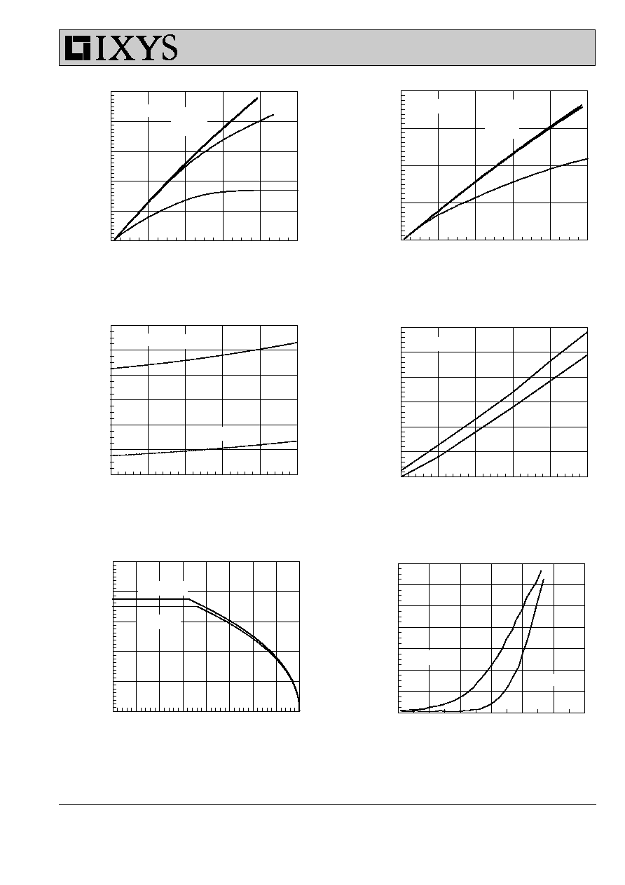
Fig.1 Output Characteristics
Fig.2
Output characteristics at elevated
temperature
Fig.3 R
DS(on)
vs. Drain Current
Fig.4
Temperature Dependence of Drain
to Source Resistance
Fig.5 Drain Current vs. Case Temperature
Fig.6
Input admittance
4 - 4
© 2000 IXYS All rights reserved
IXFH14N100
IXFT14N100
IXFX15N100
IXFH15N100
IXFT15N100
IXFX14N100
V
SD
- Volts
0.4
0.6
0.8
1.0
1.2
1.4
1.6
I
D
- A
m
per
e
s
0
8
16
24
32
40
Pulse Width - Seconds
10
-3
10
-2
10
-1
10
0
10
1
R
(th)
JC
- K
/
W
0.01
0.1
1
V
DS
- Volts
0
5
10
15
20
25
30
35
40
C
a
p
a
ci
ta
nce - pF
100
250
500
1000
2500
5000
Gate Charge - nC
0
40
80
120
160
200
240
280
V
GS
-
Volt
s
0
2
4
6
8
10
12
Vds=300V
I
D
=30A
I
G
=10mA
Crss
Coss
Ciss
V
DS
= 500V
I
D
= 7.5A
I
G
= 10mA
f = 1MHz
T
J
= 125
O
C
T
J
= 25
O
C
Single pulse
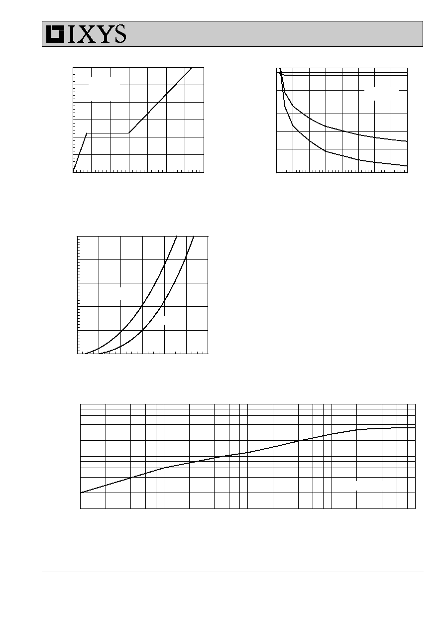
Fig.7 Gate Charge Characteristic Curve
Fig.8
Capacitance Curves
Fig.9 Source current vs Source drain voltage.
Fig.10 Transient Thermal Impedance