© 1998 IXYS All rights reserved
Symbol
Test Conditions
Maximum Ratings
V
DSS
T
J
= 25
∞
C to 150
∞
C
900
V
V
DGR
T
J
= 25
∞
C to 150
∞
C; R
GS
= 1 M
900
V
V
GS
Continuous
±
20
V
V
GSM
Transient
±
30
V
I
D25
T
C
= 25
∞
C
16
A
I
DM
T
C
= 25
∞
C, pulse width limited by T
JM
64
A
I
AR
T
C
= 25
∞
C
16
A
E
AR
T
C
= 25
∞
C
45
mJ
dv/dt
I
S
I
DM
, di/dt
100 A/
µ
s, V
DD
V
DSS
,
5
V/ns
T
J
150
∞
C, R
G
= 2
P
D
T
C
= 25
∞
C
360
W
T
J
-55 ... +150
∞
C
T
JM
150
∞
C
T
stg
-55 ... +150
∞
C
T
L
1.6 mm (0.062 in.) from case for 10 s
300
∞
C
M
d
Mounting torque
1.13/10 Nm/lb.in.
Weight
6
g
Symbol
Test Conditions
Characteristic Values
(T
J
= 25
∞
C, unless otherwise specified)
min.
typ. max.
V
DSS
V
GS
= 0 V, I
D
= 250
µ
A
900
V
V
GS(th)
V
DS
= V
GS
, I
D
= 5 mA
2.0
4.5
V
I
GSS
V
GS
=
±
20 V
DC
, V
DS
= 0
±
100
nA
I
DSS
V
DS
= 0.8 V
DSS
T
J
= 25
∞
C
25
µ
A
V
GS
= 0 V
T
J
= 125
∞
C
250
µ
A
R
DS(on)
V
GS
= 10 V, I
D
= 0.5 I
D25
0.65
Pulse test, t
300
µ
s, duty cycle d
2 %
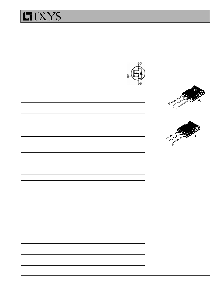
N-Channel Enhancement Mode
High dv/dt, Low t
rr
, HDMOS
TM
Family
TO-247 AD
(IXFH)
Features
l
International standard packages
l
Low R
DS (on)
HDMOS
TM
process
l
Rugged polysilicon gate cell structure
l
Unclamped Inductive Switching (UIS)
rated
l
Low package inductance
- easy to drive and to protect
l
Fast intrinsic Rectifier
Applications
l
DC-DC converters
l
Battery chargers
l
Switched-mode and resonant-mode
power supplies
l
DC choppers
l
AC motor control
l
Temperature and lighting controls
Advantages
l
Easy to mount with 1 screw (TO-247)
(isolated mounting screw hole) or
mounting clip or spring (PLUS 247
TM
)
l
Space savings
l
High power density
(TAB)
HiPerFET
TM
Power MOSFETs
97547(2/98)
PLUS 247
TM
(IXFX)
G
D
C (TAB)
Preliminary data
IXFH16N90
V
DSS
= 900 V
IXFX16N90
I
D25
= 16 A
R
DS(
on
)
= 0.65
W
t
rr
£ 200 ns

IXYS MOSFETS and IGBTs are covered by one or more of the following U.S. patents:
4,835,592 4,881,106
5,017,508
5,049,961 5,187,117 5,486,715
4,850,072 4,931,844
5,034,796
5,063,307 5,237,481 5,381,025
IXYS reserves the right to change limits, test conditions, and dimensions.
IXFH 16N90
IXFX 16N90
Symbol
Test Conditions
Characteristic Values
(T
J
= 25
∞
C, unless otherwise specified)
min.
typ. max.
g
fs
V
DS
= 10 V; I
D
= 0.5 I
D25
, pulse test
6
10
S
C
iss
4500
pF
C
oss
V
GS
= 0 V, V
DS
= 25 V, f = 1 MHz
430
pF
C
rss
150
pF
t
d(on)
27
ns
t
r
V
GS
= 10 V, V
DS
= 0.5 V
DSS
, I
D
= 0.5 I
D25
30
ns
t
d(off)
R
G
= 2
(External),
120
ns
t
f
30
ns
Q
g(on)
220
nC
Q
gs
V
GS
= 10 V, V
DS
= 0.5 V
DSS
, I
D
= 0.5 I
D25
30
nC
Q
gd
85
nC
R
thJC
0.35 K/W
R
thCK
0.25
K/W
Source-Drain Diode
Characteristic Values
(T
J
= 25
∞
C, unless otherwise specified)
Symbol
Test Conditions
min.
typ. max.
I
S
V
GS
= 0 V
16 A
I
SM
Repetitive;
64 A
pulse width limited by T
JM
V
SD
I
F
= I
S
, V
GS
= 0 V,
1.5 V
Pulse test, t
300
µ
s, duty cycle d
2 %
t
rr
T
J
= 25
∞
C
200 ns
T
J
= 125
∞
C
350 ns
Q
RM
T
J
= 25
∞
C
1
µ
C
T
J
= 125
∞
C
2
µ
C
I
RM
T
J
= 25
∞
C
10
A
T
J
= 125
∞
C
15
A
I
F
= I
S
-di/dt = 100 A/
µ
s,
V
R
= 100 V
Dim.
Millimeter
Inches
Min.
Max.
Min. Max.
A
4.7
5.3
.185
.209
A
1
2.2
2.54
.087
.102
A
2
2.2
2.6
.059
.098
b
1.0
1.4
.040
.055
b
1
1.65
2.13
.065
.084
b
2
2.87
3.12
.113
.123
C
.4
.8
.016
.031
D
20.80 21.46
.819
.845
E
15.75 16.26
.610
.640
e
5.20
5.72 0.205 0.225
L
19.81 20.32
.780
.800
L1
4.50
.177
P
3.55
3.65
.140
.144
Q
5.89
6.40 0.232 0.252
R
4.32
5.49
.170
.216
S
6.15 BSC
242 BSC
TO-247 AD (IXFH) Outline
Terminals: 1 - Gate
2 - Drain
3 - Source
Tab - Drain
1 2 3
PLUS 247
TM
Outline