© 2004 IXYS All rights reserved
Symbol
Test Conditions
Maximum Ratings
V
DSS
T
J
= 25
∞C to 150∞C
1200
V
V
DGR
T
J
= 25
∞C to 150∞C; R
GS
= 1 M
1200
V
V
GS
Continuous
±30
V
V
GSM
Transient
±40
V
I
D25
T
C
= 25
∞C
24
A
I
DM
T
C
= 25
∞C, pulse width limited by T
JM
96
A
I
AR
T
C
= 25
∞C
12
A
E
AR
T
C
= 25
∞C
30
mJ
E
AS
T
C
= 25
∞C
4.0
J
dv/dt
I
S
I
DM
, di/dt
100 A/µs, V
DD
V
DSS
,
20
V/ns
T
J
150∞C, R
G
= 2
P
D
T
C
= 25
∞C
830
W
T
J
-55 ... +150
∞C
T
JM
150
∞C
T
stg
-55 ... +150
∞C
T
L
1.6 mm (0.063 in) from case for 10 s
300
∞C
M
d
Mounting torque
TO-264
0.9/6 Nm/lb.in.
Weight
PLUS-247
6
g
TO-264
10
g
HiPerFET
TM
Power MOSFETs
Q-Class
N-Channel Enhancement Mode
Avalanche Rated, High dv/dt, Low Q
g
Low intrinsic R
g
, low t
rr
Features
Double metal process for low gate
resistance
International standard packages
Epoxy
meet
UL
94
V-0, flammability
classification
Avalanche energy and current rated
Fast intrinsic Rectifier
Advantages
Easy to mount
Space savings
High power density
Symbol
Test Conditions
Characteristic Values
(T
J
= 25
∞C, unless otherwise specified)
min.
typ.
max.
V
DSS
V
GS
= 0 V, I
D
= 3mA
1200
V
V
GS(th)
V
DS
= V
GS
, I
D
= 8 mA
2.5
5.0
V
I
GSS
V
GS
=
±30 V
DC
, V
DS
= 0
±200 nA
I
DSS
V
DS
= V
DSS
T
J
= 25
∞C
50
µA
V
GS
= 0 V
T
J
= 125
∞C
2 mA
R
DS(on)
V
GS
= 10 V, I
D
= 0.5 ∑ I
D25
0.65
Pulse test, t
300 µs, duty cycle d 2 %
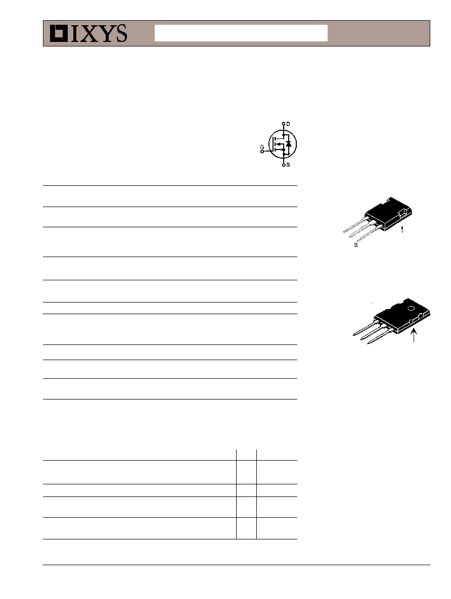
G = Gate
D = Drain
S = Source
TAB = Drain
DS99185(05/04)
TO-264 AA (IXFK)
S
G
D
D (TAB)
V
DSS
= 1200 V
I
D25
=
24 A
R
DS(on)
= 0.65
t
rr
300 ns
IXFK 24N120Q2
IXFX 24N120Q2
PLUS 247
TM
(IXFX)
G
D
D (TAB)
Preliminary Data Sheet
Advance Technical Data
IXYS reserves the right to change limits, test conditions, and dimensions.
IXYS MOSFETs and IGBTs are covered by one or more
4,850,072
4,931,844
5,034,796
5,063,307
5,237,481
5,381,025
6,404,065B1 6,162,665
6,534,343
6,583,505
of the following U.S. patents:
4,835,592
4,881,106
5,017,508
5,049,961
5,187,117
5,486,715
6,306,728B1
6,259,123B1 6,306,728B1 6,683,344
Symbol
Test Conditions
Characteristic Values
(T
J
= 25
∞C, unless otherwise specified)
min.
typ.
max.
g
fs
V
DS
= 20 V; I
D
= 0.5 ∑ I
D25
, pulse test
15
25
S
C
iss
8200
pF
C
oss
V
GS
= 0 V, V
DS
= 25 V, f = 1 MHz
560
pF
C
rss
110
pF
t
d(on)
22
ns
t
r
V
GS
= 10 V, V
DS
= 0.5 ∑ V
DSS
, I
D
= 0.5 ∑ I
D25
13
ns
t
d(off)
R
G
= 1.0
(External),
60
ns
t
f
12
ns
Q
g(on)
180
nC
Q
gs
V
GS
= 10 V, V
DS
= 0.5 ∑ V
DSS
, I
D
= 0.5 ∑ I
D25
45
nC
Q
gd
80
nC
R
thJC
0.15
K/W
R
thCK
TO-264
0.15
K/W
Source-Drain Diode
Characteristic Values
(T
J
= 25
∞C, unless otherwise specified)
Symbol
Test Conditions
min.
typ. max.
I
S
V
GS
= 0 V
24
A
I
SM
Repetitive; pulse width limited by T
JM
96
A
V
SD
I
F
= I
S
, V
GS
= 0 V,
1.5
V
Pulse test, t
300 µs, duty cycle d 2 %
t
rr
300 ns
Q
RM
1
µC
I
RM
10
A
I
F
= 25A, -di/dt = 100 A/
µs, V
R
= 100 V
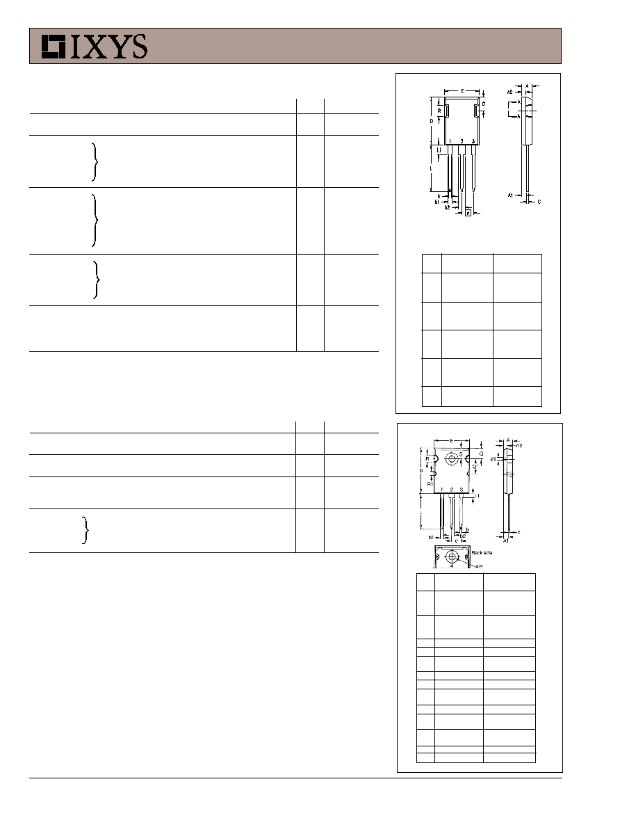
TO-264 AA Outline
Millimeter
Inches
Min.
Max.
Min.
Max.
A
4.82
5.13
.190
.202
A1
2.54
2.89
.100
.114
A2
2.00
2.10
.079
.083
b
1.12
1.42
.044
.056
b1
2.39
2.69
.094
.106
b2
2.90
3.09
.114
.122
c
0.53
0.83
.021
.033
D
25.91
26.16
1.020
1.030
E
19.81
19.96
.780
.786
e
5.46 BSC
.215 BSC
J
0.00
0.25
.000
.010
K
0.00
0.25
.000
.010
L
20.32
20.83
.800
.820
L1
2.29
2.59
.090
.102
P
3.17
3.66
.125
.144
Q
6.07
6.27
.239
.247
Q1
8.38
8.69
.330
.342
R
3.81
4.32
.150
.170
R1
1.78
2.29
.070
.090
S
6.04
6.30
.238
.248
T
1.57
1.83
.062
.072
Dim.
IXFK 24N120Q2
IXFX 24N120Q2
Dim.
Millimeter
Inches
Min.
Max.
Min. Max.
A
4.83
5.21
.190
.205
A
1
2.29
2.54
.090
.100
A
2
1.91
2.16
.075
.085
b
1.14
1.40
.045
.055
b
1
1.91
2.13
.075
.084
b
2
2.92
3.12
.115
.123
C
0.61
0.80
.024
.031
D
20.80
21.34
.819
.840
E
15.75
16.13
.620
.635
e
5.45 BSC
.215 BSC
L
19.81
20.32
.780
.800
L1
3.81
4.32
.150
.170
Q
5.59
6.20
.220 0.244
R
4.32
4.83
.170
.190
Terminals: 1 - Gate
2 - Drain (Collector)
3 - Source (Emitter)
4 - Drain (Collector)
PLUS 247
TM
Outline