© 2001 IXYS All rights reserved
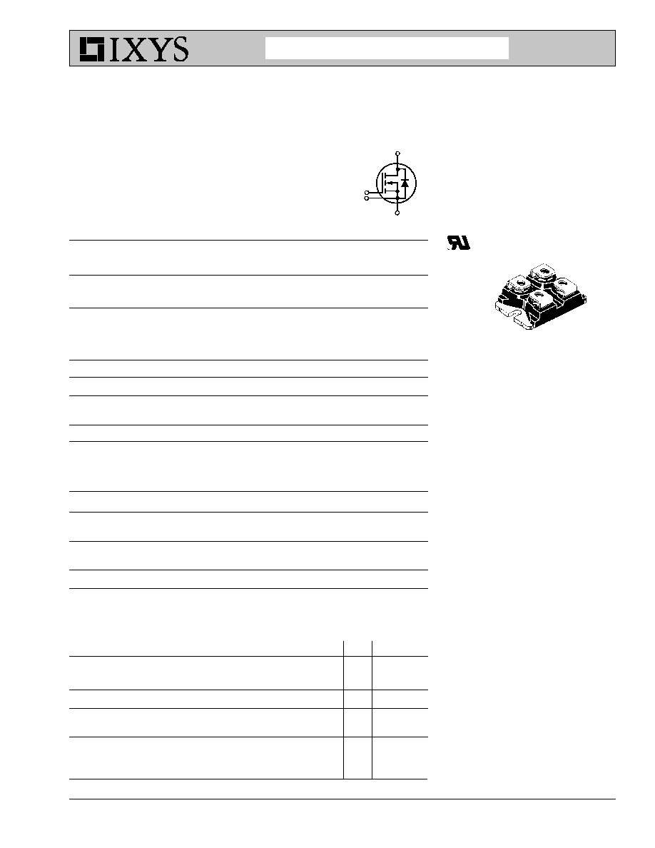
Symbol
Test Conditions
Characteristic Values
(T
J
= 25
∞
C, unless otherwise specified)
min.
typ.
max.
V
DSS
V
GS
= 0 V, I
D
= 1 mA
500
V
V
GH(th)
V
DS
= V
GS
, I
D
= 8 mA
3.0
5.5
V
I
GSS
V
GS
=
±
20 V
DC
, V
DS
= 0
±
200
nA
I
DSS
V
DS
= V
DSS
T
J
= 25
∞
C
100
µ
A
V
GS
= 0 V
T
J
= 125
∞
C
3
mA
R
DS(on)
V
GS
= 10 V, I
D
= 0.5 I
D25
Pulse test, t
300
µ
s, duty cycle d
2 %
85
m
Symbol
Test Conditions
Maximum Ratings
V
DSS
T
J
= 25
∞
C to 150
∞
C
500
V
V
DGR
T
J
= 25
∞
C to 150
∞
C; R
GS
= 1 M
500
V
V
GS
Continuous
±
20
V
V
GSM
Transient
±
3
0
V
I
D25
T
C
= 25
∞
C
55
A
I
DM
T
C
= 25
∞
C, pulse width limited by T
JM
220
A
I
AR
T
C
= 25
∞
C
55
A
E
AR
T
C
= 25
∞
C
60
mJ
E
AS
T
C
= 25
∞
C
3
.0
J
dv/dt
I
S
I
DM
, di/dt
100 A/
µ
s, V
DD
V
DSS
,
5
V/ns
T
J
150
∞
C, R
G
= 2
P
D
T
C
= 25
∞
C
600
W
T
J
-55 ... +150
∞
C
T
JM
150
∞
C
T
stg
-55 ... +150
∞
C
T
J
1.6 mm (0.63 in) from case for 10 s
-
∞
C
V
ISOL
50/60 Hz, RMS
t = 1 min
2500
V~
I
ISOL
1 mA
t = 1 s
3000
V~
M
d
Mounting torque
1.5/13Nm/lb.in.
Terminal connection torque
1.5/13Nm/lb.in.
Weight
3
0
g
98854 (8/01)
D
S
G
S
S
G
S
D
miniBLOC, SOT-227 B
E153432
G = Gate
D = Drain
S = Source
Either Source terminal at miniBLOC can be used
as Main or Kelvin Source
Advance Technical Information
IXFN 55N50F
V
DSS
=
500 V
I
D25
=
55
A
R
DS(on)
= 85 m
t
rr
250 ns
HiPerRF
TM
Power MOSFETs
F-Class: MegaHertz Switching
N-Channel Enhancement Mode
Avalanche Rated,
Low Q
g,
Low Intrinsic R
g
High dV/dt,
Low t
rr
Features
l
RF capable Mosfets
l
Rugged polysilicon gate cell structure
l
Double metal process for low gate
resistance
l
Unclamped Inductive Switching (UIS)
rated
l
Low package inductance
- easy to drive and to protect
l
Fast intrinsic rectifier
Applications
l
DC-DC converters
l
Switched-mode and resonant-mode
power supplies, >500kHz switching
l
DC choppers
l
Pulse generation
l
Laser drivers
Advantages
l
Easy to mount
l
Space savings
l
High power density
IXYS MOSFETS and IGBTs are covered by one or more of the following U.S. patents:
4,835,592
4,881,106
5,017,508
5,049,961
5,187,117
5,486,715
4,850,072
4,931,844
5,034,796
5,063,307
5,237,481
5,381,025
IXYS reserves the right to change limits, test conditions, and dimensions.
IXFN 55N50F
Symbol
Test Conditions
Characteristic Values
(T
J
= 25
∞
C, unless otherwise specified)
min.
typ.
max.
g
fs
V
DS
= 10 V; I
D
= 0.5 ∑ I
D25
, pulse test
22
33
S
C
iss
6700
pF
C
oss
V
GS
= 0 V, V
DS
= 25 V, f = 1 MHz
1250
pF
C
rss
330
pF
t
d(on)
24
ns
t
r
V
GS
= 10 V, V
DS
= 0.5 ∑ V
DSS
, I
D
= 0.5 ∑ I
D25
20
ns
t
d(off)
R
G
= 1
(External),
45
ns
t
f
9.6
ns
Q
g(on)
195
nC
Q
gs
V
GS
= 10 V, V
DS
= 0.5 ∑ V
DSS
, I
D
= 0.5 ∑ I
D25
50
nC
Q
gd
95
nC
R
thJC
0.21
K/W
R
thCK
0.05
K/W
Source-Drain Diode
Characteristic Values
(T
J
= 25
∞
C, unless otherwise specified)
Symbol
Test Conditions
min.
typ.
max.
I
S
V
GS
= 0 V
55
A
I
SM
Repetitive;
220
A
pulse width limited by T
JM
V
SD
I
F
= I
S
, V
GS
= 0 V,
1.5
V
Pulse test, t
300
µ
s, duty cycle d
2 %
t
rr
I
F
= 50A, -di/dt = 100 A/
µ
s, V
R
= 100 V
250
ns
Q
RM
1.6
µ
C
I
RM
13
A
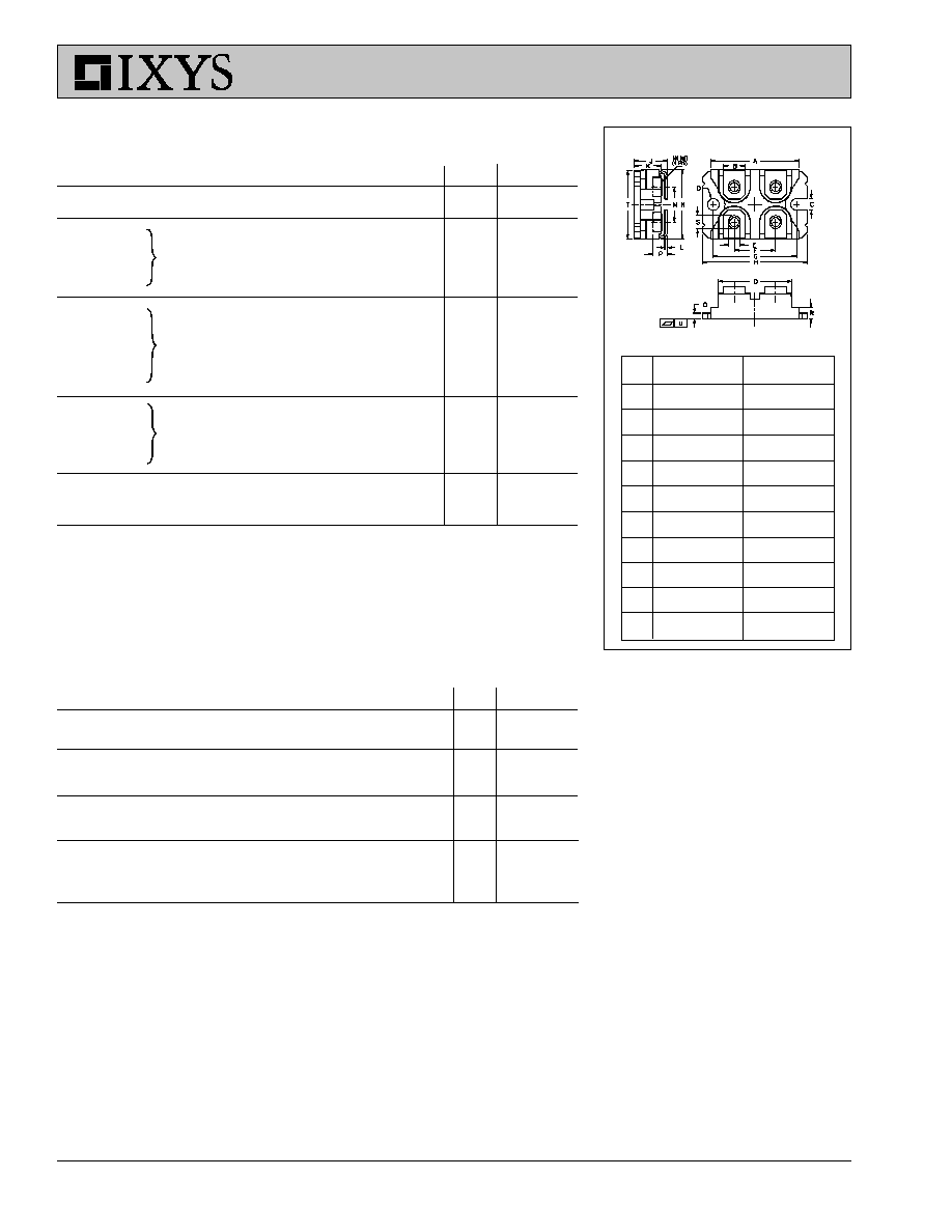
miniBLOC, SOT-227 B
M4 screws (4x) supplied
Dim.
Millimeter
Inches
Min.
Max.
Min.
Max.
A
31.50
31.88
1.240
1.255
B
7.80
8.20
0.307
0.323
C
4.09
4.29
0.161
0.169
D
4.09
4.29
0.161
0.169
E
4.09
4.29
0.161
0.169
F
14.91
15.11
0.587
0.595
G30.12
30.30
1.186
1.193
H
38.00
38.23
1.496
1.505
J
11.68
12.22
0.460
0.481
K
8.92
9.60
0.351
0.378
L
0.76
0.84
0.030
0.033
M
12.60
12.85
0.496
0.506
N
25.15
25.42
0.990
1.001
O
1.98
2.13
0.078
0.084
P
4.95
5.97
0.195
0.235
Q
26.54
26.90
1.045
1.059
R
3.94
4.42
0.155
0.174
S
4.72
4.85
0.186
0.191
T
24.59
25.07
0.968
0.987
U
-0.05
0.1
-0.002
0.004