© 2004 IXYS All rights reserved
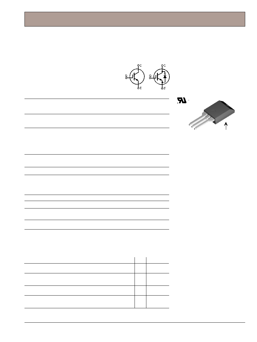
G = Gate
C = Collector
E = Emitter
Symbol
Test Conditions
Maximum Ratings
V
CES
T
J
= 25
∞C to 150∞C
600
V
V
CGR
T
J
= 25
∞C to 150∞C; R
GE
= 1 M
600
V
V
GES
Continuous
±20
V
V
GEM
Transient
±30
V
I
C25
T
C
= 25
∞C
20
A
I
C110
T
C
= 110
∞C
8
A
I
D110
T
C
= 110
∞C (IXGC16N60C2D1 diode)
10
A
I
CM
T
C
= 25
∞C, 1 ms
100
A
SSOA
V
GE
= 15 V, T
J
= 125
∞C, R
G
= 22
I
CM
= 32
A
(RBSOA)
Clamped inductive load
@0.8 V
CES
P
C
T
C
= 25
∞C
63
W
T
J
-55 ... +150
∞C
T
JM
150
∞C
T
stg
-55 ... +150
∞C
F
C
Mounting Force
11..65/2.5..15
N/lb.
V
ISOL
Isolation Voltage; 50/60Hz; t = 1minute; RMS
2500
V
Maximum lead temperature for soldering
300
∞C
1.6 mm (0.062 in.) from case for 10 s
Weight
2
g
Symbol
Test Conditions
Characteristic Values
(T
J
= 25
∞C, unless otherwise specified)
min.
typ.
max.
V
GE(th)
I
C
= 250
µA, V
CE
= V
GE
2.5
5.0
V
I
CES
V
CE
= V
CES
16N60C2
25
µA
V
GE
= 0 V
16N60C2D1
50
µA
I
GES
V
CE
= 0 V, V
GE
=
±20 V
±100
nA
V
CE(sat)
I
C
= 12 A
,
V
GE
= 15 V
2.7
3.0
V
Note 2
T
J
=125
∞C
2.1
V
DS99149A(11/04)
HiPerFAST
TM
IGBT
C2-Class High Speed
IGBT in ISOPLUS220
TM
Case
Electrically Isolated Back Surface
IXGC 16N60C2
IXGC 16N60C2D1
V
CES
= 600 V
I
C25
=
20 A
V
CE(sat)
= 3.0 V
t
fi(typ)
=
35 ns
D1
G
C
E
ISOPLUS 220
TM
(IXGC)
Isolated back surface*
Features
DCB Isolated mounting tab
UL recognized (E153432)
Meets TO-273 package Outline
High current handling capability
MOS Gate turn-on
- drive simplicity
Epoxy meets UL94V-0 flammability
classification
Applications
Uninterruptible power supplies (UPS)
Switched-mode and resonant-mode
power supplies
AC motor speed control
DC servo and robot drives
DC choppers
Advantages
Easy assembly
High power density
Very fast switching speeds for high
frequency applications
E153432
Preliminary Data Sheet
IXYS reserves the right to change limits, test conditions, and dimensions.
IXGC 16N60C2
IXGC 16N60C2D1
IXYS MOSFETs and IGBTs are covered by
4,835,592
4,931,844
5,049,961
5,237,481
6,162,665
6,404,065 B1
6,683,344
6,727,585
one or moreof the following U.S. patents:
4,850,072
5,017,508
5,063,307
5,381,025
6,259,123 B1
6,534,343
6,710,405B2
6,759,692
4,881,106
5,034,796
5,187,117
5,486,715
6,306,728 B1
6,583,505
6,710,463
Symbol
Test Conditions
Characteristic Values
(T
J
= 25
∞C, unless otherwise specified)
min.
typ.
max.
g
fs
I
C
= 12A; V
CE
= 10 V,
8
12
S
Note 2.
C
ies
V
CE
= 25 V, V
GE
= 0 V, f = 1 MHz
720
pF
C
oes
16N60C2
55
pF
16N60C2D1
65
pF
C
res
19
pF
Q
g
I
C
= 20A, V
GE
= 15 V, V
CE
= 0.5 V
CES
32
nC
Q
ge
6
nC
Q
gc
10
nC
t
d(on)
25
ns
t
ri
15
ns
t
d(off)
60
120
ns
t
fi
35
100
ns
E
off
60
100
µJ
t
d(on)
25
ns
t
ri
18
ns
E
on
16N60C2D1
0.38
mJ
t
d(off)
115
ns
t
fi
70
ns
E
off
150
µJ
R
thJC
2.0 K/W
R
thCK
0.25
K/W
Inductive load, T
J
= 125
∞∞
∞∞
∞C
I
C
= 12A; V
GE
= 15 V
V
CE
= 400 V; R
G
= R
off
= 22
Note 1
Inductive load, T
J
= 25
∞∞
∞∞
∞C
I
C
= 12 A; V
GE
= 15 V
V
CE
= 400 V; R
G
= R
off
= 22
Note 1.
Notes:
1. Switching times may increase for V
CE
(Clamp) > 0.8 ∑ V
CES
, higher T
J
,
or increased R
G
.
2. Pulse test, t
300 µs, duty cycle d 2 %
Reverse Diode (FRED)
Characteristic Values
(T
J
= 25
∞C, unless otherwise specified)
Symbol
Test Conditions
min. typ. max.
V
F
I
F
= 10 A, V
GE
= 0 V
2.66
V
T
J
= 125
∞C
1.66
V
I
RM
I
F
= 12 A; -di
F
/dt = 100 A/
µs, V
R
= 100 V
2.5
A
t
rr
V
GE
= 0 V; T
J
= 125
∞C
110
ns
t
rr
I
F
= 1 A; -di
F
/dt = 100 A/
µs; V
R
= 30 V, V
GE
= 0 V
30
ns
R
thJC
2.5 K/W
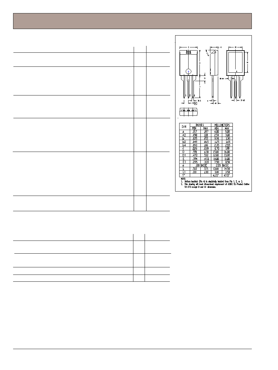
ISOPLUS220 Outline