© 1997 IXYS All rights reserved
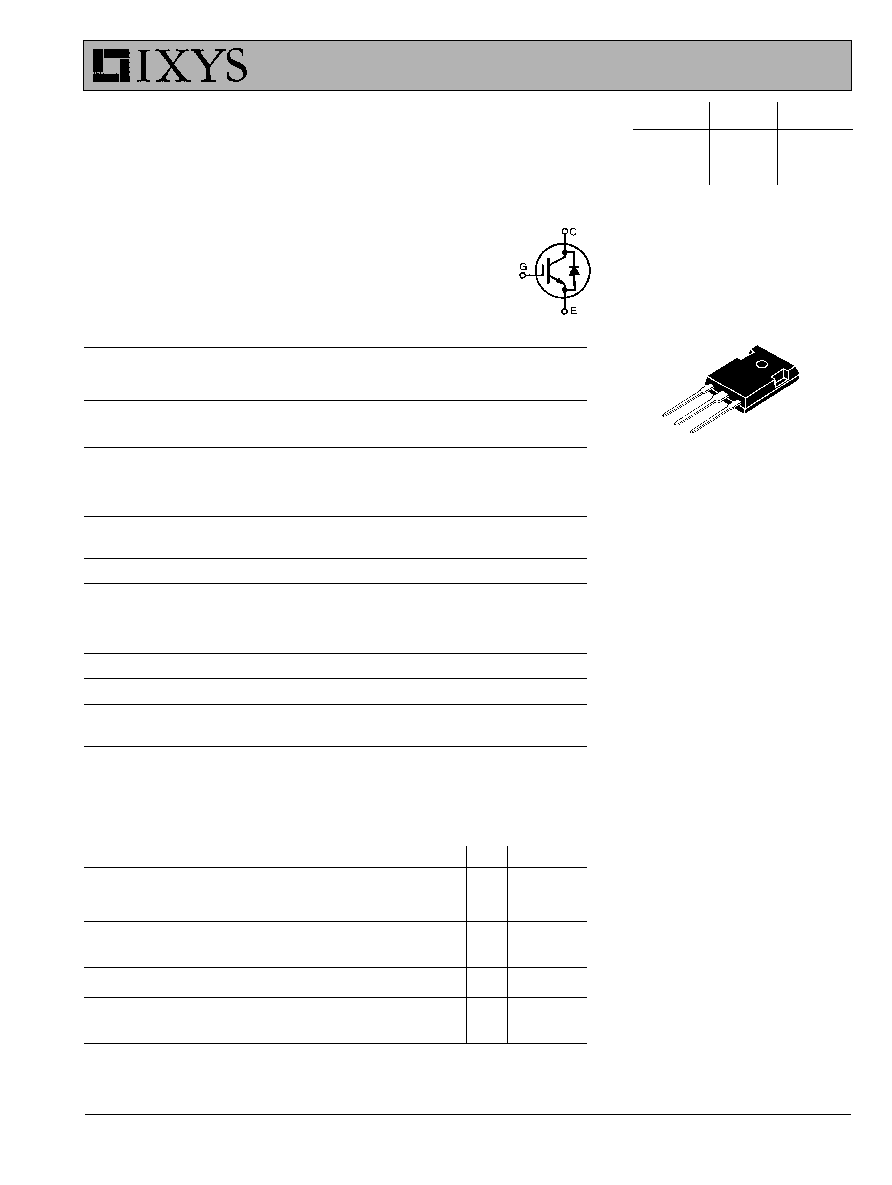
TO-247 AD
G
C
E
G = Gate,
C = Collector,
E = Emitter,
TAB = Collector
Symbol
Test Conditions
Maximum Ratings
V
CES
T
J
= 25
∞
C to 150
∞
C
1000
V
V
CGR
T
J
= 25
∞
C to 150
∞
C; R
GE
= 1 M
1000
V
V
GES
Continuous
±
20
V
V
GEM
Transient
±
30
V
I
C25
T
C
= 25
∞
C
20
A
I
C90
T
C
= 90
∞
C
10
A
I
CM
T
C
= 25
∞
C, 1 ms
40
A
SSOA
V
GE
= 15 V, T
VJ
= 125
∞
C, R
G
= 150
I
CM
= 20
A
(RBSOA)
Clamped inductive load, L = 300
µ
H
@ 0.8 V
CES
P
C
T
C
= 25
∞
C
100
W
T
J
-55 ... +150
∞
C
T
JM
150
∞
C
T
stg
-55 ... +150
∞
C
M
d
Mounting torque (M3)
1.13/10 Nm/lb.in.
Weight
6
g
Maximum lead temperature for soldering
300
∞
C
1.6 mm (0.062 in.) from case for 10 s
Symbol
Test Conditions
Characteristic Values
(T
J
= 25
∞
C, unless otherwise specified)
min.
typ.
max.
BV
CES
I
C
= 4 mA, V
GE
= 0 V
1000
V
V
GE(th)
I
C
= 500
µ
A, V
CE
= V
GE
2.5
5.5
V
I
CES
V
CE
= 0.8 ∑ V
CES
T
J
= 25
∞
C
400
µ
A
V
GE
= 0 V
T
J
= 125
∞
C
5
mA
I
GES
V
CE
= 0 V, V
GE
=
±
20 V
±
100
nA
V
CE(sat)
I
C
= I
C90
, V
GE
= 15 V
10N100U1
3.5
V
10N100AU1
4.0
V
V
CES
I
C25
V
CE(sat)
Low V
CE(sat)
IGBT with Diode
IXGH
10
N100U1
1000 V
20 A
3.5 V
High speed IGBT with Diode
IXGH
10
N100AU1
1000 V
20 A
4.0 V
Combi Packs
Features
l
International standard package
JEDEC TO-247 AD
l
IGBT and anti-parallel FRED in one
package
l
2nd generation HDMOS
TM
process
l
Low V
CE(sat)
- for low on-state conduction losses
l
MOS Gate turn-on
- drive simplicity
l
Fast Recovery
Epitaxial Diode (FRED)
- soft recovery with low I
RM
Applications
l
AC motor speed control
l
DC servo and robot drives
l
DC choppers
l
Uninterruptible power supplies (UPS)
l
Switch-mode and resonant-mode
power supplies
Advantages
l
Space savings (two devices in one
package)
l
Easy to mount with 1 screw
(isolated mounting screw hole)
l
Reduces assembly time and cost
91753F (3/97)
IXYS MOSFETS and IGBTs are covered by one or more of the following U.S. patents:
4,835,592
4,881,106
5,017,508
5,049,961
5,187,117
5,486,715
4,850,072
4,931,844
5,034,796
5,063,307
5,237,481
5,381,025
IXYS reserves the right to change limits, test conditions, and dimensions.
IXGH 10N100U1
IXGH 10N100AU1
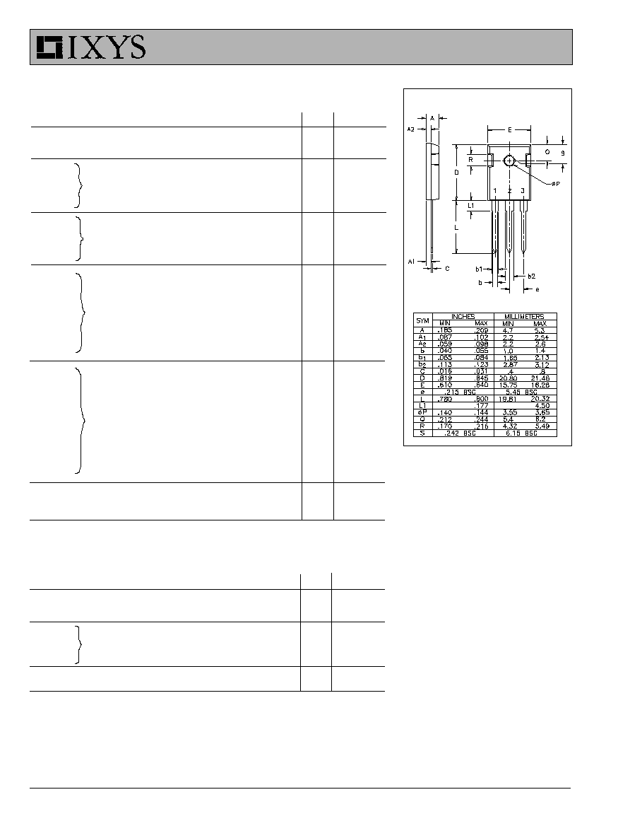
TO-247 AD Outline
Symbol
Test Conditions
Characteristic Values
(T
J
= 25
∞
C, unless otherwise specified)
min.
typ.
max.
g
fs
I
C
= I
C90
; V
CE
= 10 V,
4
8
S
Pulse test, t
300
µ
s, duty cycle
2 %
C
ies
750
pF
C
oes
V
CE
= 25 V, V
GE
= 0 V, f = 1 MHz
200
pF
C
res
30
pF
Q
g
52
70
nC
Q
ge
I
C
= I
C90
, V
GE
= 15 V, V
CE
= 0.5 V
CES
13
25
nC
Q
gc
24
45
nC
t
d(on)
100
ns
t
ri
200
ns
t
d(off)
550
900
ns
t
fi
10N100U1
800
ns
10N100AU1
500
ns
E
off
10N100AU1
2
3
mJ
t
d(on)
100
ns
t
ri
200
ns
E
on
1.1
mJ
t
d(off)
600
1000
ns
t
fi
10N100U1
1250
2000
ns
10N100AU1
600
1000
ns
E
off
10N100U1
5.0
mJ
10N100AU1
2.5
mJ
R
thJC
1.2 K/W
R
thCK
0.25
K/W
Reverse Diode (FRED)
Characteristic Values
(T
J
= 25
∞
C, unless otherwise specified)
Symbol
Test Conditions
min.
typ.
max.
V
F
I
F
= I
C90
, V
GE
= 0 V,
2.75
V
Pulse test, t
300
µ
s, duty cycle d
2 %
I
RM
I
F
= I
C90
, V
GE
= 0 V, -di
F
/dt = 100 A/
µ
s
6.5
A
t
rr
V
R
= 540 V
T
J
= 125
∞
C
120
ns
I
F
= 1 A; -di/dt = 50 A/
µ
s; V
R
= 30 V T
J
= 25
∞
C
50
60
ns
R
thJC
1.6 K/W
Inductive load, T
J
= 125
∞∞
∞∞
∞
C
I
C
= I
C90
, V
GE
= 15 V, L = 300
µ
H
V
CE
= 0.8 V
CES
, R
G
= R
off
= 150
Remarks: Switching times
may increase
for V
CE
(Clamp) > 0.8 ∑ V
CES
,
higher T
J
or increased R
G
Inductive load, T
J
= 25
∞∞
∞∞
∞
C
I
C
= I
C90
, V
GE
= 15 V, L = 300
µ
H,
V
CE
= 0.8 V
CES
, R
G
= R
off
= 150
Remarks: Switching times
may increase
for V
CE
(Clamp) > 0.8 ∑ V
CES
,
higher T
J
or increased R
G
1 = Gate
2 = Collector
3 = Emitter
Tab = Collector
© 1997 IXYS All rights reserved
IXGH 10N100U1
IXGH 10N100AU1
T
J
- Degrees C
-50
-25
0
25
50
75
100 125 150
B
V
/
V
(t
h
)
-
No
rm
alize
d
0.5
0.6
0.7
0.8
0.9
1.0
1.1
1.2
1.3
T
J
- Degrees C
-50
-25
0
25
50
75
100 125 150
V
(sa
t
)
-
No
rma
lize
d
0.7
0.8
0.9
1.0
1.1
1.2
1.3
1.4
1.5
V
CE
- Volts
0
1
2
3
4
5
I
C
- Am
pe
res
0
2
4
6
8
10
12
14
16
18
20
T
J
= 25∞C
V
GE
= 15V
7V
9V
11V
V
GE
- Volts
5
6
7
8
9
10
11
12
13 14
15
V
CE
-
Vo
lts
0
1
2
3
4
5
6
7
8
9
10
V
GE
- Volts
0
1
2
3
4
5
6
7
8
9
10
I
C
- A
m
p
ere
s
0
2
4
6
8
10
12
14
16
18
20
V
CE
- Volts
0
2
4
6
8
10
12
14
16
18
20
I
C
-
Am
pe
res
0
10
20
30
40
50
60
70
80
13V
11V
9V
7V
13V
T
J
= 25∞C
V
GE
= 15V
I
C
= 5A
I
C
= 10A
I
C
= 20A
V
GE
= 15V
I
C
= 5A
I
C
= 10A
V
CE
= 10V
T
J
= 125∞C
T
J
= 25∞C
T
J
= - 40∞C
V
GE(th)
I
C
= 250µA
BV
CES
I
C
= 3mA
10N100p1.JNB
T
J
= 25∞C
I
C
= 20A
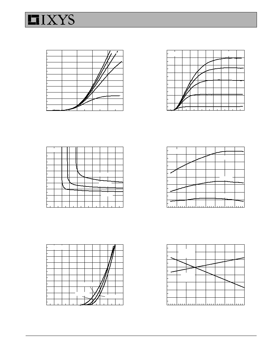
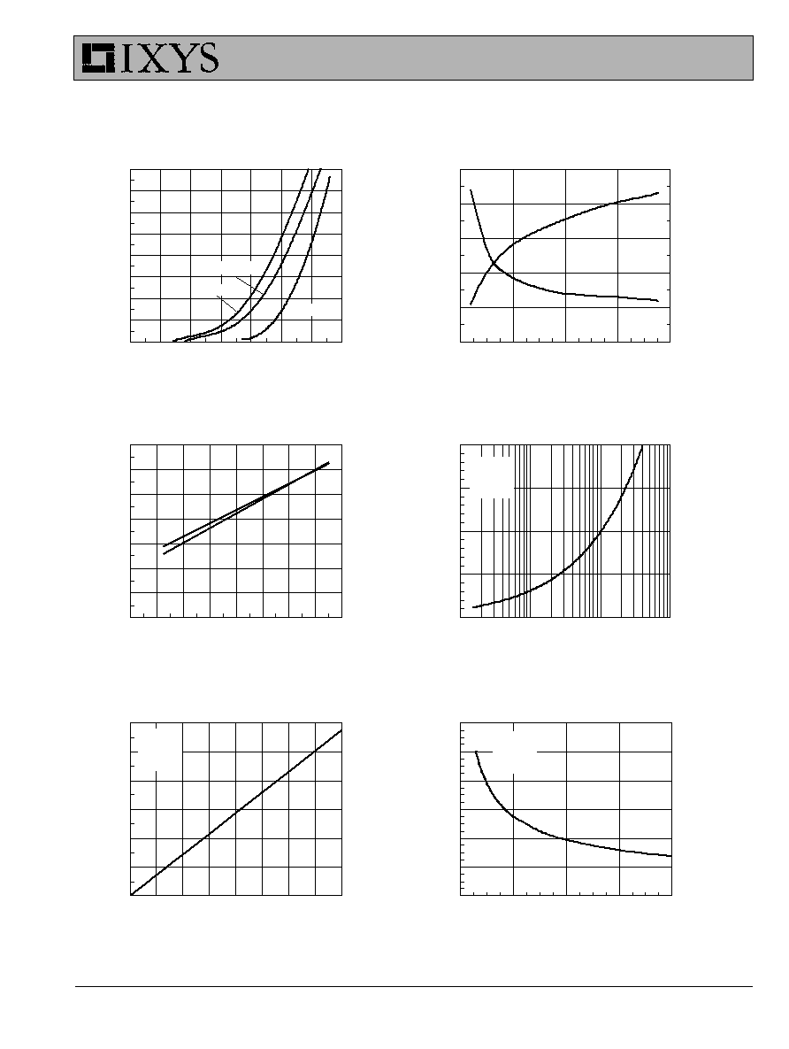
Fig. 3 Collector-Emitter Voltage
Fig. 4 Temperature Dependence
vs. Gate-Emitter Voltage
of Output Saturation Voltage
Fig. 5 Input Admittance
Fig. 6 Temperature Dependence of
Breakdown and Threshold Voltage
Fig. 1 Saturation Characteristics
Fig. 2 Output Characterstics
IXYS MOSFETS and IGBTs are covered by one or more of the following U.S. patents:
4,835,592
4,881,106
5,017,508
5,049,961
5,187,117
5,486,715
4,850,072
4,931,844
5,034,796
5,063,307
5,237,481
5,381,025
IXYS reserves the right to change limits, test conditions, and dimensions.
IXGH 10N100U1
IXGH 10N100AU1
I
C
- Amperes
4
6
8
10
12
14
16
18
20
22
t
fi
- nan
os
eco
nds
600
650
700
750
800
850
900
E
of
f
- m
illij
oule
s
1
2
3
4
5
6
7
R
G
- Ohms
20
40
60
80
100
120
140
160
E
of
f
-
mil
lijou
les
0
1
2
3
4
5
t
fi
- na
no
sec
ond
s
0
200
400
600
800
1000
Time - Seconds
0.00001
0.0001
0.001
0.01
0.1
1
T
h
e
rma
l R
esp
ons
e -
K/W
0.01
0.1
1
V
CE
- Volts
0
200
400
600
800
1000
I
C
-
Am
pe
res
0.01
0.1
1
10
T
J
= 125∞C
R
G
= 150
dV/dt < 3V/ns
Q
g
- nCoulombs
0
10
20
30
40
50
V
GE
- Vol
ts
0
3
6
9
12
15
tfi
Eoff
tfi
Eoff
D=0.1
D=0.2
Single Pulse
D = Duty Cycle
D=0.01
I
C
= 10A
I
C
= 10A
V
CE
= 800V
R
G
=150
TJ =125∞C
T
J
=125∞C
D=0.05
D=0.02
D=0.5
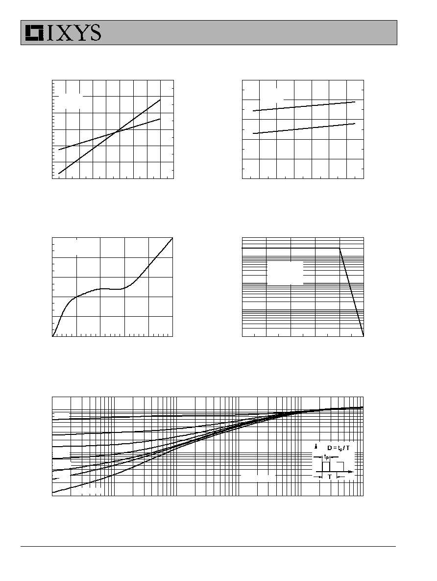
Fig.11 Transient Thermal Impedance
Fig.9 Gate Charge Characteristic Curve Fig.10 Turn-Off Safe Operating Area
Fig.7 Turn-Off Energy per Pulse and Fig.8 Dependence of Turn-Off Energy
Fall Time on Collector Current
Per Pulse and Fall Time on R
G
© 1997 IXYS All rights reserved
IXGH 10N100U1
IXGH 10N100AU1
di
F
/dt - A/µs
0
100
200
300
400
t
rr
-
nano
sec
ond
s
0
100
200
300
400
500
600
di
F
/dt - A/µs
100
200
300
400
I
RM
-
A
m
per
es
0
5
10
15
20
25
30
di
F
/dt - A/µs
1
10
100
1000
Q
r
-
n
anoc
oul
o
m
b
s
0.0
0.5
1.0
1.5
2.0
T
J
- Degrees C
0
20
40
60
80
100
120
140
160
N
o
r
m
a
liz
e
d
I
RM
/Q
r
0.0
0.2
0.4
0.6
0.8
1.0
1.2
1.4
Q
r
I
RM
di
F
/dt - A/µs
0
100
200
300
400
t
fr
-
n
ano
sec
ond
s
0
200
400
600
800
1000
V
FR
- V
o
l
t
s
0
10
20
30
40
50
t
fr
V
FR
T
J
= 125∞C
I
F
= 12A
Voltage Drop - Volts
0.0
0.5
1.0
1.5
2.0
2.5
3.0
3.5
C
u
r
r
e
n
t
- A
m
p
e
re
s
0
5
10
15
20
25
30
35
40
T
J
= 150∞C
T
J
= 100∞C
V
R
= 540V
I
F
= 12A
T
J
= 100∞C
T
J
= 25∞C
T
J
= 100∞C
V
R
= 540V
I
F
= 12A
T
J
= 100∞C
V
R
= 540V
I
F
= 12A
Fig.14 Junction Temperature Dependence Fig.15 Reverse Recovery Chargee
off I
RM
and Q
r
Fig.16 Peak Reverse Recovery Current Fig.17 Reverse Recovery Time
Fig.12 Maximum Forward Voltage Drop Fig.13 Peak Forward Voltage V
FR
and
Forward Recovery Time t
FR
IXYS MOSFETS and IGBTs are covered by one or more of the following U.S. patents:
4,835,592
4,881,106
5,017,508
5,049,961
5,187,117
5,486,715
4,850,072
4,931,844
5,034,796
5,063,307
5,237,481
5,381,025
IXYS reserves the right to change limits, test conditions, and dimensions.
IXGH 10N100U1
IXGH 10N100AU1
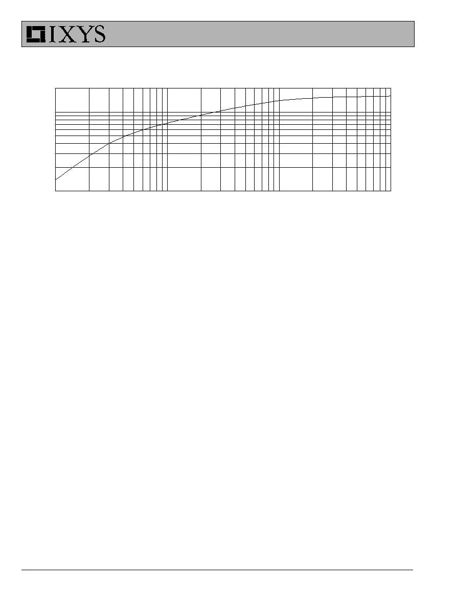
Fig.18 Diode Transient Thermal resistance junction to case
Pulse Width - Seconds
0.001
0.003
0.01
0.1
R
th
J
C
-
K/
W
0.1
1.0