© 2003 IXYS All rights reserved
V
CES
= 1700
V
I
C25
= 50
A
V
CE(sat)
= 3.3
V
t
fi(typ)
= 290 ns
IXGH 24N170
IXGT 24N170
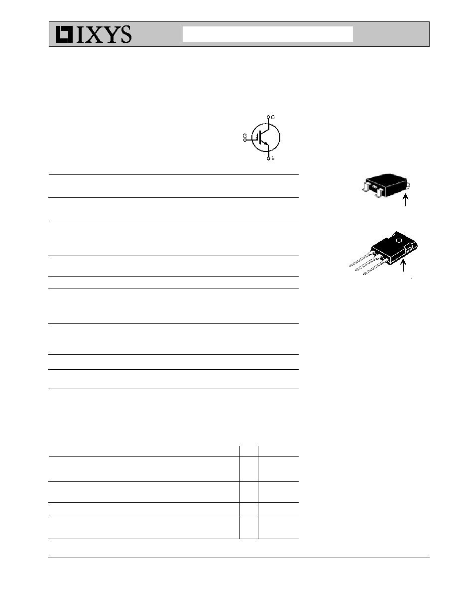
C (TAB)
G = Gate,
C = Collector,
E = Emitter,
TAB = Collector
G
C
E
TO-247 AD
(IXGH)
Features
International standard packages
JEDEC TO-268 and
JEDEC TO-247 AD
High current handling capability
MOS Gate turn-on
- drive simplicity
Rugged NPT structure
Molding epoxies meet UL
94
V-0
flammability classification
Applications
Capacitor discharge & pulser circuits
AC motor speed control
DC servo and robot drives
DC choppers
Uninterruptible power supplies (UPS)
Switched-mode and resonant-mode
power supplies
Advantages
High power density
Suitable for surface mounting
Easy to mount with 1 screw,
(isolated mounting screw hole)
DS98994(01/03)
Symbol
Test Conditions
Characteristic Values
(T
J
= 25
∞
C, unless otherwise specified)
min.
typ.
max.
BV
CES
I
C
= 250
µ
A, V
GE
= 0 V
1700
V
V
GE(th)
I
C
= 250
µ
A, V
CE
= V
GE
3.0
5.0
V
I
CES
V
CE
= 0.8 ∑ V
CES
T
J
= 25
∞
C
50
µ
A
V
GE
= 0 V
T
J
= 125
∞
C
500
µ
A
I
GES
V
CE
= 0 V, V
GE
=
±
20 V
±
100
nA
V
CE(sat)
I
C
= I
C90
, V
GE
= 15 V
T
J
= 25
∞
C
2.5
3.3
V
T
J
= 125
∞
C
3.0
V
Symbol
Test Conditions
Maximum Ratings
V
CES
T
J
= 25
∞
C to 150
∞
C
1700
V
V
CGR
T
J
= 25
∞
C to 150
∞
C; R
GE
= 1 M
1700
V
V
GES
Continuous
±
20
V
V
GEM
Transient
±
30
V
I
C25
T
C
= 25
∞
C
50
A
I
C90
T
C
= 90
∞
C
24
A
I
CM
T
C
= 25
∞
C, 1 ms
150
A
SSOA
V
GE
= 15 V, T
VJ
= 125
∞
C, R
G
= 5
I
CM
= 50
A
(RBSOA)
Clamped inductive load
@ 0.8 V
CES
P
C
T
C
= 25
∞
C
250
W
T
J
-55 ... +150
∞
C
T
JM
150
∞
C
T
stg
-55 ... +150
∞
C
Maximum Lead temperature for soldering
300
∞
C
1.6 mm (0.062 in.) from case for 10 s
Maximum Tab temperature for soldering SMD devices for 10 s
260
∞
C
M
d
Mounting torque (M3)
1.13/10Nm/lb.in.
Weight
TO-247 AD
6
g
TO-268
4
g
TO-268 (IXGT)
G
E
High Voltage
IGBT
C (TAB)
Advance Technical Data
IXYS reserves the right to change limits, test conditions, and dimensions.
IXYS MOSFETs and IGBTs are covered by one or more of the following U.S. patents:
4,835,592
4,881,106
5,017,508
5,049,961
5,187,117
5,486,715
6,306,728B1
4,850,072
4,931,844
5,034,796
5,063,307
5,237,481
5,381,025
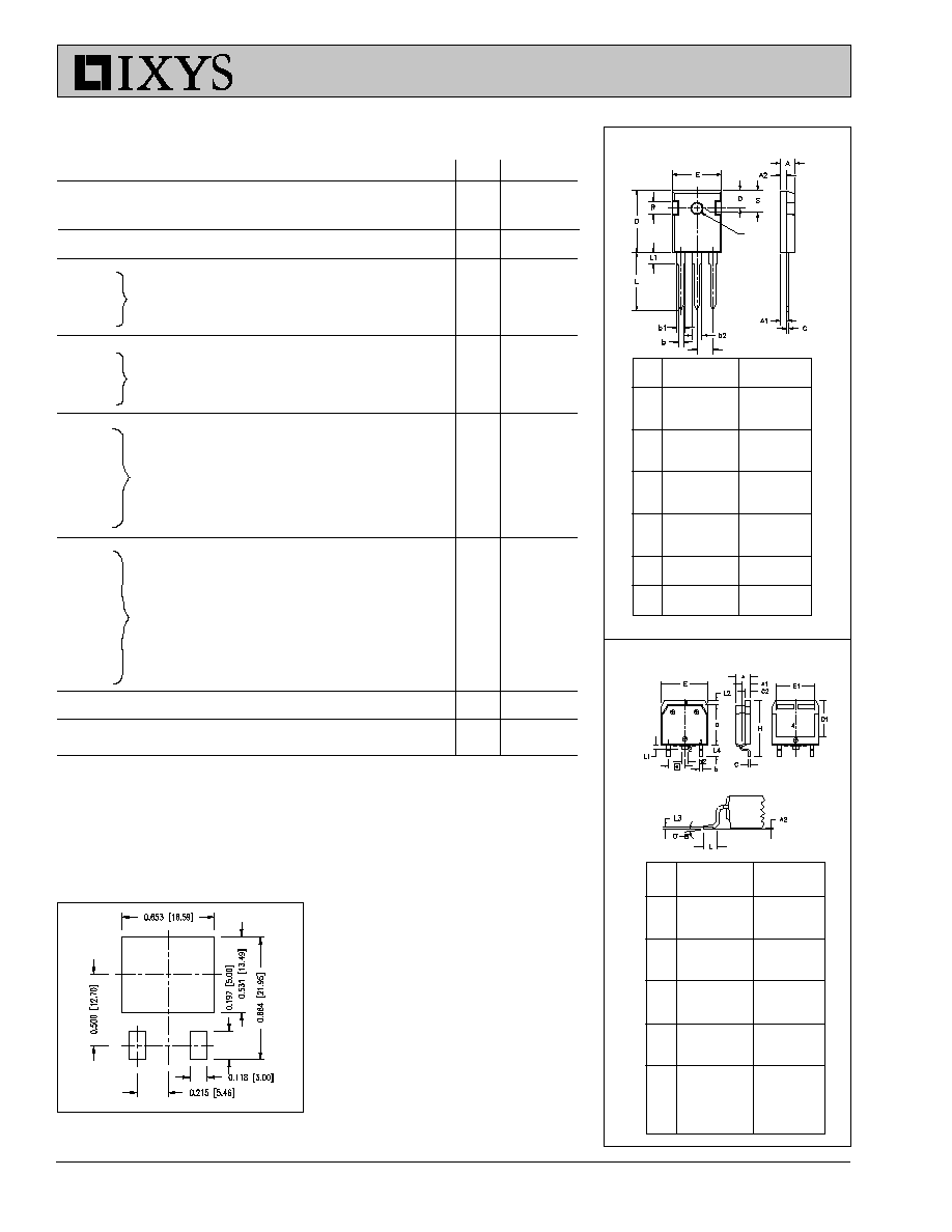
Dim.
Millimeter
Inches
Min.
Max.
Min. Max.
A
4.7
5.3
.185
.209
A
1
2.2
2.54
.087
.102
A
2
2.2
2.6
.059
.098
b
1.0
1.4
.040
.055
b
1
1.65
2.13
.065
.084
b
2
2.87
3.12
.113
.123
C
.4
.8
.016
.031
D
20.80
21.46
.819
.845
E
15.75
16.26
.610
.640
e
5.20
5.72
0.205 0.225
L
19.81
20.32
.780
.800
L1
4.50
.177
P
3.55
3.65
.140
.144
Q
5.89
6.40
0.232 0.252
R
4.32
5.49
.170
.216
S
6.15 BSC
242 BSC
e
P
TO-247 AD Outline
Remarks: Switching times may
increase for V
CE
(Clamp) > 0.8 ∑ V
CES
,
higher T
J
or increased R
G
Remarks: Switching times may
increase for V
CE
(Clamp) > 0.8 ∑ V
CES
,
higher T
J
or increased R
G
Symbol
Test Conditions
Characteristic Values
(T
J
= 25
∞
C, unless otherwise specified)
min.
typ.
max.
g
fs
I
C
= I
C90
; V
CE
= 10 V,
18
25
S
Pulse test, t
300
µ
s, duty cycle
2 %
I
C(ON)
V
GE
= 10V, V
CE
= 10V
100
A
C
ies
2400
pF
C
oes
V
CE
= 25 V, V
GE
= 0 V, f = 1 MHz
120
pF
C
res
33
pF
Q
g
106
nC
Q
ge
I
C
= I
C90
, V
GE
= 15 V, V
CE
= 0.5 V
CES
18
nC
Q
gc
32
nC
t
d(on)
42
ns
t
ri
39
ns
t
d(off)
200
400
ns
t
fi
250
500
ns
E
off
8
12 mJ
t
d(on)
50
ns
t
ri
55
ns
E
on
2.0
mJ
t
d(off)
200
ns
t
fi
360
ns
E
off
12
mJ
R
thJC
0.5 K/W
R
thCK
(TO-247)
0.25
K/W
Inductive load, T
J
= 125
∞∞
∞∞
∞
C
I
C
= I
C25
, V
GE
= 15 V
V
CE
= 0.8 V
CES
, R
G
= R
off
= 5
Inductive load, T
J
= 25
∞∞
∞∞
∞
C
I
C
= I
C25
, V
GE
= 15 V
V
CE
= 0.8 V
CES
, R
G
= R
off
= 5
Min Recommended Footprint
IXGH 24N170
IXGT 24N170
TO-268 Outline
Dim.
Millimeter
Inches
Min.
Max.
Min. Max.
A
4.9
5.1
.193
.201
A
1
2.7
2.9
.106
.114
A
2
.02
.25
.001
.010
b
1.15
1.45
.045
.057
b
2
1.9
2.1
.75
.83
C
.4
.65
.016
.026
D
13.80
14.00
.543
.551
E
15.85
16.05
.624
.632
E
1
13.3
13.6
.524
.535
e 5.45 BSC .215 BSC
H
18.70
19.10
.736
.752
L
2.40
2.70
.094
.106
L1
1.20
1.40
.047
.055
L2
1.00
1.15
.039
.045
L3 0.25 BSC .010 BSC
L4
3.80
4.10
.150
.161