© 2003 IXYS All rights reserved
DS95567C(02/03)
Symbol
Test Conditions
Characteristic Values
(T
J
= 25
∞
C, unless otherwise specified)
min.
typ.
max.
BV
CES
I
C
= 750
µ
A, V
GE
= 0 V
600
V
V
GE(th)
I
C
= 250
µ
A, V
CE
= V
GE
2.5
5.0
V
I
CES
V
CE
= 0.8 ∑ V
CES
T
J
= 25
∞
C
500
µ
A
V
GE
= 0 V
T
J
= 125
∞
C
8
mA
I
GES
V
CE
= 0 V, V
GE
=
±
20 V
±
100
nA
V
CE(sat)
I
C
= I
C90
, V
GE
= 15 V
2.3
V
Symbol
Test Conditions
Maximum Ratings
V
CES
T
J
= 25
∞
C to 150
∞
C
600
V
V
CGR
T
J
= 25
∞
C to 150
∞
C; R
GE
= 1 M
600
V
V
GES
Continuous
±
20
V
V
GEM
Transient
±
30
V
I
C25
T
C
= 25
∞
C
60
A
I
C90
T
C
= 90
∞
C
32
A
I
CM
T
C
= 25
∞
C, 1 ms
120
A
SSOA
V
GE
= 15 V, T
VJ
= 125
∞
C, R
G
= 33
I
CM
= 64
A
(RBSOA)
Clamped inductive load, L = 100
µ
H
@ 0.8 V
CES
P
C
T
C
= 25
∞
C
200
W
T
J
-55 ... +150
∞
C
T
JM
150
∞
C
T
stg
-55 ... +150
∞
C
Maximum Lead and Tab temperature for soldering
300
∞
C
1.6 mm (0.062 in.) from case for 10 s
M
d
Mounting torque, TO-247 AD
1.13/10
Nm/lb.in.
Weight
6
g
HiPerFAST
TM
IGBT
with Diode
Features
International standard packages
JEDEC TO-247 SMD
High frequency IGBT and antiparallel
FRED in one package
High current handling capability
Newest generation HDMOS
TM
process
MOS Gate turn-on
- drive simplicity
Applications
AC motor speed control
DC servo and robot drives
DC choppers
Uninterruptible power supplies (UPS)
Switched-mode and resonant-mode
power supplies
Advantages
Space savings (two devices in one
package)
High power density
Very fast switching speeds for high
frequency applications
IXGH 32N60BU1
V
CES
= 600 V
I
C25
= 60 A
V
CE(sat)
= 2.3 V
t
fi
= 80 ns
C (TAB)
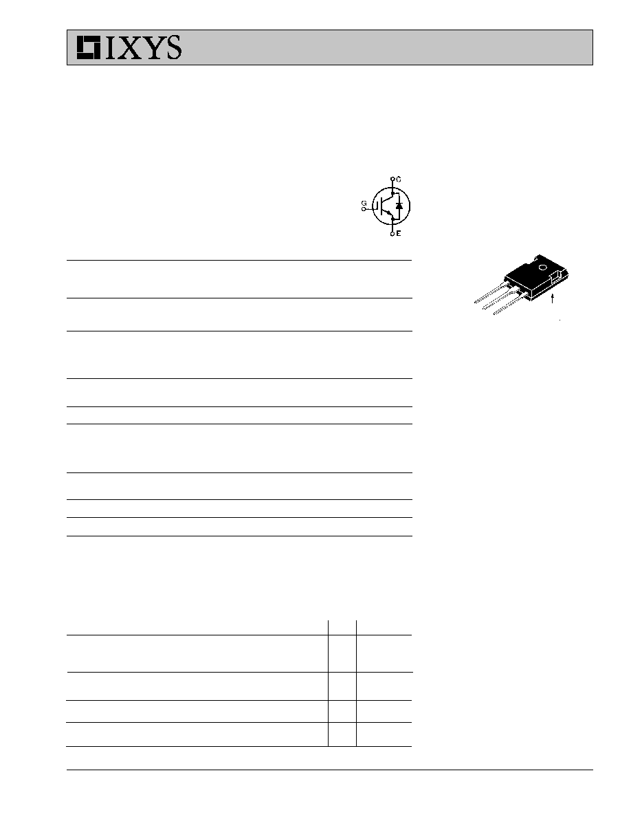
G = Gate,
C = Collector,
E = Emitter,
TAB = Collector
G
C
E
TO-247 AD
IXYS reserves the right to change limits, test conditions, and dimensions.
IXYS MOSFETS and IGBTs are covered by one or more of the following U.S. patents:
4,835,592
4,881,106
5,017,508
5,049,961
5,187,117
5,486,715
6,306,728B1
4,850,072
4,931,844
5,034,796
5,063,307
5,237,481
5,381,025
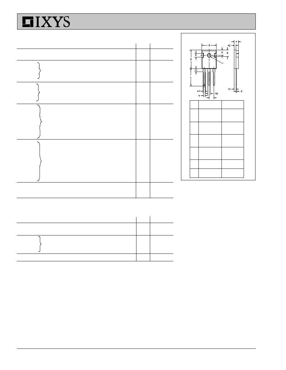
TO-247 AD Outline
Dim.
Millimeter
Inches
Min.
Max.
Min. Max.
A
4.7
5.3
.185
.209
A
1
2.2
2.54
.087
.102
A
2
2.2
2.6
.059
.098
b
1.0
1.4
.040
.055
b
1
1.65
2.13
.065
.084
b
2
2.87
3.12
.113
.123
C
.4
.8
.016
.031
D
20.80
21.46
.819
.845
E
15.75
16.26
.610
.640
e
5.20
5.72
0.205 0.225
L
19.81
20.32
.780
.800
L1
4.50
.177
P
3.55
3.65
.140
.144
Q
5.89
6.40
0.232 0.252
R
4.32
5.49
.170
.216
S
6.15 BSC
242 BSC
e
P
Symbol
Test Conditions
Characteristic Values
(T
J
= 25
∞
C, unless otherwise specified)
min.
typ.
max.
g
fs
I
C
= I
C90
; V
CE
= 10 V,
15
25
S
Pulse test, t
300
µ
s, duty cycle
2 %
C
ies
2700
pF
C
oes
V
CE
= 25 V, V
GE
= 0 V, f = 1 MHz
270
pF
C
res
50
pF
Q
G
110
150 nC
Q
GE
I
C
= I
C90
, V
GE
= 15 V, V
CE
= 0.5 V
CES
23
35 nC
Q
GC
40
75 nC
t
d(on)
25
ns
t
ri
20
ns
t
d(off)
100
200
ns
t
fi
80
150
ns
E
off
0.6
1.2 mJ
t
d(on)
25
ns
t
ri
25
ns
E
on
1
mJ
t
d(off)
120
ns
t
fi
120
ns
E
off
1.2
mJ
R
thJC
0.62 K/W
R
thCK
0.25
K/W
Reverse Diode (FRED)
Characteristic Values
(T
J
= 25
∞
C, unless otherwise specified)
Symbol
Test Conditions
min.
typ.
max.
V
F
I
F
= I
C90
, V
GE
= 0 V,
1.6
V
Pulse test, t
300
µ
s, duty cycle d
2 %
I
RM
I
F
= I
C90
, V
GE
= 0 V, -di
F
/dt = 240 A/
µ
s
10
15
A
t
rr
V
R
= 360 V
T
J
= 125
∞
C 150
ns
I
F
= 1 A; -di/dt = 100 A/
µ
s; V
R
= 30 V T
J
= 25
∞
C
35
50
ns
R
thJC
1 K/W
Inductive load, T
J
= 25
∞∞
∞∞
∞
C
I
C
= I
C90
, V
GE
= 15 V, L = 100
µ
H,
V
CE
= 0.8 V
CES
, R
G
= R
off
= 4.7
Remarks: Switching times may
increase for V
CE
(Clamp) > 0.8 ∑ V
CES
,
higher T
J
or increased R
G
Inductive load, T
J
= 125
∞∞
∞∞
∞
C
I
C
= I
C90
, V
GE
= 15 V, L = 100
µ
H
V
CE
= 0.8 V
CES
, R
G
= R
off
= 4.7
Remarks: Switching times may
increase for V
CE
(Clamp) > 0.8 ∑ V
CES
,
higher T
J
or increased R
G
IXGH32N60BU1

© 2003 IXYS All rights reserved
IXGH32N60BU1
T
J
- Degrees C
-50 -25
0
25
50
75 100 125 150
B
V/
V
GE
(t
h
)
- N
o
rm
a
liz
e
d
0.70
0.75
0.80
0.85
0.90
0.95
1.00
1.05
1.10
1.15
T
J
- Degrees C
25
50
75
100
125
150
V
CE (s
a
t
)
- No
rma
l
i
z
e
d
0.75
1.00
1.25
1.50
1.75
V
CE
- Volts
0
1
2
3
4
5
6
7
I
C
-
A
m
per
es
0
20
40
60
80
100
V
GE
- Volts
3
4
5
6
7
8
9
10
I
C
-
A
m
per
es
0
20
40
60
80
100
V
CE
- Volts
0
2
4
6
8
10
I
C
-
Am
per
es
0
40
80
120
160
200
13V
11V
9V
7V
V
CE
= 10V
V
GE
= 15V
13V
11V
9V
7V
T
J
= 25∞C
V
GE
= 15V
T
J
= 25∞C
I
C
= 16A
I
C
= 32A
I
C
= 64A
T
J
=
125∞C
V
GE(th)
I
C
= 250µA
BV
CES
I
C
= 250µA
G32N60B P1
5V
5V
V
GE
= 15V
T
J
= 25∞C
V
CE
- Volts
0
1
2
3
4
5
6
7
I
C
-
Am
per
es
0
20
40
60
80
100
T
J
= 125∞C
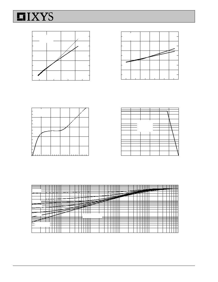
Fig. 6. Temperature Dependence of BV
DSS
& V
GE(th)
Fig. 5. Admittance Curves
Fig. 3. Saturation Voltage Characteristics
Fig. 4. Temperature Dependence of V
CE(sat)
Fig. 1. Saturation Voltage Characteristics
Fig. 2. Extended Output Characteristics
IXYS reserves the right to change limits, test conditions, and dimensions.
IXYS MOSFETS and IGBTs are covered by one or more of the following U.S. patents:
4,835,592
4,881,106
5,017,508
5,049,961
5,187,117
5,486,715
6,306,728B1
4,850,072
4,931,844
5,034,796
5,063,307
5,237,481
5,381,025
Fig. 11. Transient Thermal Resistance
Pulse Width - Seconds
0.00001
0.0001
0.001
0.01
0.1
1
Z
th
JC
(
K
/W
)
0.001
0.01
0.1
1
D=0.2
V
CE
- Volts
0
100
200
300
400
500
600
I
C
-
Am
per
es
0.1
1
10
100
Q
g
- nanocoulombs
0
25
50
75
100
125
150
V
GE
-
Vol
t
s
0
3
6
9
12
15
R
G
- Ohms
0
10
20
30
40
50
60
E
(O
F
F
)
-
m
i
llij
ou
les
0
1
2
3
4
5
E
(O
N)
-
m
i
l
lij
ou
les
0.0
0.5
1.0
1.5
2.0
2.5
T
J
= 125∞C
I
C
- Amperes
0
20
40
60
80
E
(
O
FF)
-
m
ill
iJ
oule
s
0
1
2
3
4
5
E
(O
N)
-
m
ill
ij
oul
es
0.0
0.5
1.0
1.5
2.0
2.5
V
CE
= 300V
I
C
= 32A
I
C
= 32A
E
(ON)
E
(OFF)
E
(ON)
E
(OFF)
T
J
= 125∞C
R
G
= 4.7
dV/dt < 5V/ns
D=0.5
D=0.1
D=0.05
D=0.02
D=0.01
Single pulse
D = Duty Cycle
R
G
= 10
T
J
= 125∞C
Fig. 10. Turn-off Safe Operating Area
Fig. 9. Gate Charge
Fig. 8. Dependence of tfi and E
OFF
on R
G
.
Fig. 7. Dependence of tfi and E
OFF
on I
C
.
IXGH32N60BU1
© 2003 IXYS All rights reserved
IXGH32N60BU1
di
F
/dt - A/µs
0
200
400
600
t
rr
-
na
nosecond
s
0.0
0.2
0.4
0.6
0.8
di
F
/dt - A/µs
200
400
600
I
RM
-
Am
per
es
0
10
20
30
40
di
F
/dt - A/µs
1
10
100
1000
Q
r
-
n
anocoul
om
bs
0
1
2
3
4
T
J
- Degrees C
0
40
80
120
160
N
o
r
m
al
i
z
ed I
RM
/Q
r
0.0
0.2
0.4
0.6
0.8
1.0
1.2
1.4
Q
r
I
RM
di
F
/dt - A/µs
0
100
200
300
400
500
600
t
fr
-
n
anoseco
nds
0
200
400
600
800
1000
V
FR
- V
o
lts
0
5
10
15
20
25
t
fr
V
FR
Voltage Drop - Volts
0.5
1.0
1.5
2.0
2.5
C
u
r
r
en
t
-
Am
per
es
0
20
40
60
80
100
T
J
= 150∞C
T
J
= 100∞C
T
J
= 25∞C
T
J
= 125∞C
I
F
= 37A
typ.
I
F
= 60A
I
F
= 30A
I
F
= 15A
I
F
= 30A
T
J
= 100∞C
V
R
= 350V
T
J
= 100∞C
V
R
= 350V
T
J
= 100∞C
V
R
= 350V
typ.
I
F
= 60A
I
F
= 30A
I
F
= 15A
max.
I
F
= 30A
max.
I
F
= 30A
typ.
I
F
= 60A
I
F
= 30A
I
F
= 15A
max.
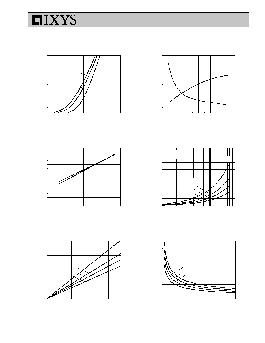
Fig.14 Junction Temperature Dependence
Fig.15 Reverse Recovery Chargee
off I
RM
and Q
r
Fig.16 Peak Reverse Recovery Current
Fig.17 Reverse Recovery Time
Fig.12 Maximum Forward Voltage Drop
Fig.13 Peak Forward Voltage V
FR
and
Forward Recovery Time t
FR