© 2005 IXYS All rights reserved
DS99329(02/05)
PolarHV
TM
Power MOSFET
IXTA 14N60P
V
DSS
= 600 V
IXTP 14N60P
I
D25
= 14 A
IXTQ 14N60P
R
DS(on)
550 m
N-Channel Enhancement Mode
Features
International standard packages
Unclamped Inductive Switching (UIS)
rated
Low package inductance
- easy to drive and to protect
Advantages
Easy to mount
Space savings
High power density
Symbol
Test Conditions
Characteristic Values
(T
J
= 25
∞
C, unless otherwise specified)
Min. Typ.
Max.
V
DSS
V
GS
= 0 V, I
D
= 250
µ
A
600
V
V
GS(th)
V
DS
= V
GS
, I
D
= 250
µ
A
3.0
5.0
V
I
GSS
V
GS
=
±
30 V
DC
, V
DS
= 0
±
100
nA
I
DSS
V
DS
= V
DSS
25
µ
A
V
GS
= 0 V
T
J
= 125
∞
C
250
µ
A
R
DS(on)
V
GS
= 10 V, I
D
= 0.5 I
D25
550 m
Pulse test, t
300
µ
s, duty cycle d
2 %
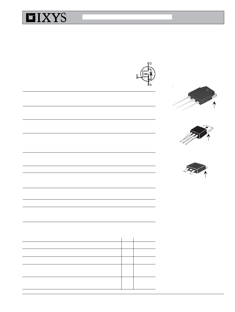
G = Gate
D = Drain
S = Source
TAB = Drain
TO-3P (IXTQ)
TO-263 (IXTA)
TO-220 (IXTP)
G
D
S
(TAB)
D
(TAB)
G
S
G
S
(TAB)
ADVANCE TECHNICAL INFORMATION
Symbol
Test Conditions
Maximum Ratings
V
DSS
T
J
= 25
∞
C to 150
∞
C
600
V
V
DGR
T
J
= 25
∞
C to 150
∞
C; R
GS
= 1 M
600
V
V
GS
Continuous
±
30
V
V
GSM
Tranisent
±
40
V
I
D25
T
C
= 25
∞
C
14
A
I
DM
T
C
= 25
∞
C, pulse width limited by T
JM
42
A
I
AR
T
C
= 25
∞
C
14
A
E
AR
T
C
= 25
∞
C
23
mJ
E
AS
T
C
= 25
∞
C
0.9
J
dv/dt
I
S
I
DM
, di/dt
100 A/
µ
s, V
DD
V
DSS
,
10
V/ns
T
J
150
∞
C, R
G
= 4
P
D
T
C
= 25
∞
C
300
W
T
J
-55 ... +150
∞
C
T
JM
150
∞
C
T
stg
-55 ... +150
∞
C
T
L
1.6 mm (0.062 in.) from case for 10 s
300
∞
C
Plastic body for 10 s
250
∞
C
M
d
Mounting torque
(TO-3P,TO-220)
1.13/10 Nm/lb.in.
Weight
TO-3P
5.5
g
TO-220
4
g
TO-263 2 g

IXYS reserves the right to change limits, test conditions, and dimensions.
IXTP 14N60P
IXTQ 14N60P
t
rr
I
F
= 18A
-di/dt = 100 A/
µ
s
V
R
= 100V
Q
RM
510
4.0
ns
µ
C
TO-3P (IXTQ) Outline
IXYS MOSFETs and IGBTs are covered by
4,835,592
4,931,844
5,049,961
5,237,481
6,162,665
6,404,065 B1
6,683,344
6,727,585
one or moreof the following U.S. patents:
4,850,072
5,017,508
5,063,307
5,381,025
6,259,123 B1
6,534,343
6,710,405B2
6,759,692
4,881,106
5,034,796
5,187,117
5,486,715
6,306,728 B1
6,583,505
6,710,463
Dim.
Millimeter
Inches
Min.
Max.
Min.
Max.
A
4.06
4.83
.160
.190
A1
2.03
2.79
.080
.110
b
0.51
0.99
.020
.039
b2
1.14
1.40
.045
.055
c
0.46
0.74
.018
.029
c2
1.14
1.40
.045
.055
D
8.64
9.65
.340
.380
D1
7.11
8.13
.280
.320
E
9.65
10.29
.380
.405
E1
6.86
8.13
.270
.320
e
2.54
BSC
.100
BSC
L
14.61
15.88
.575
.625
L1
2.29
2.79
.090
.110
L2
1.02
1.40
.040
.055
L3
1.27
1.78
.050
.070
L4
0
0.38
0
.015
R
0.46
0.74
.018
.029
TO-263 (IXTA) Outline
Pins: 1 - Gate
2 - Drain
TO-220 (IXTP) Outline
Symbol
Test Conditions
Characteristic Values
(T
J
= 25
∞
C, unless otherwise specified)
Min.
Typ. Max.
g
fs
V
DS
= 20 V; I
D
= 0.5 I
D25
, pulse test
9
13
S
C
iss
2200
pF
C
oss
V
GS
= 0 V, V
DS
= 25 V, f = 1 MHz
210
pF
C
rss
27
pF
t
d(on)
23
ns
t
r
V
GS
= 10 V, V
DS
= 0.5 V
DSS
, I
D
= I
D25
27
ns
t
d(off)
R
G
= 10
(External)
70
ns
t
f
26
ns
Q
g(on)
70
nC
Q
gs
V
GS
= 10 V, V
DS
= 0.5 V
DSS
, I
D
= 0.5 I
D25
17
nC
Q
gd
34
nC
R
thJC
0.42 K/W
R
thCK
(TO-3P)
0.21
K/W
R
thCK
(TO-220)
0.25
K/W
Source-Drain Diode
Characteristic Values
(T
J
= 25
∞
C, unless otherwise specified)
Symbol
Test Conditions
min.
typ.
max.
I
S
V
GS
= 0 V
14
A
I
SM
Repetitive
42
A
V
SD
I
F
= I
S
, V
GS
= 0 V,
1.5
V
Pulse test, t
300
µ
s, duty cycle d
2 %
IXTA 14N60P