
© 2004 IXYS All rights reserved
Symbol
Test Conditions
Maximum Ratings
V
DSS
T
J
= 25
∞C to 175∞C
60
V
V
DGR
T
J
= 25
∞C to 175∞C; R
GS
= 1 M
55
V
V
GS
Continuous
±20
V
V
GSM
Transient
±30
V
I
D25
T
C
= 25
∞C
150
A
I
DRMS
External lead current limit
75
A
I
DM
T
C
= 25
∞C, pulse width limited by T
JM
280
A
I
AR
T
C
= 25
∞C
60
A
E
AR
T
C
= 25
∞C
40
mJ
E
AS
T
C
= 25
∞C
1.0
J
dv/dt
I
S
I
DM
, di/dt
100 A/µs, V
DD
V
DSS
,
10
V/ns
T
J
150∞C, R
G
= 10
P
D
T
C
= 25
∞C
480
W
T
J
-55 ... +175
∞C
T
JM
175
∞C
T
stg
-55 ... +150
∞C
T
L
1.6 mm (0.062 in.) from case for 10 s
300
∞C
Maximum tab temperature for soldering
260
∞C
package for 10s
M
d
Mounting torque
1.13/10 Nm/lb.in.
Weight
5.5
g
G = Gate
D = Drain
S = Source
TAB = Drain
DS99254(11/04)
Symbol
Test Conditions
Characteristic Values
(T
J
= 25
∞C, unless otherwise specified)
Min. Typ.
Max.
V
DSS
V
GS
= 0 V, I
D
= 250
µA
60
V
V
GS(th)
V
DS
= V
GS
, I
D
= 250
µA
2.5
5.0
V
I
GSS
V
GS
=
±20 V
DC
, V
DS
= 0
±100
nA
I
DSS
V
DS
= V
DSS
25
µA
V
GS
= 0 V
T
J
= 150
∞C
250
µA
R
DS(on)
V
GS
= 10 V, I
D
= 0.5 I
D25
8
10
m
Pulse test, t
300 µs, duty cycle d 2 %
PolarHT
TM
Power MOSFET
Advanced Technical Information
N-Channel Enhancement Mode
Features
International standard packages
Unclamped Inductive Switching (UIS)
rated
Low package inductance
- easy to drive and to protect
Advantages
Easy to mount
Space savings
High power density
TO-3P (IXTQ)
G
D
S
(TAB)
IXTQ 150N06P
V
DSS
= 60 V
I
D25
= 150 A
R
DS(on)
= 10 m

IXYS reserves the right to change limits, test conditions, and dimensions.
IXTQ 150N06P
IXYS MOSFETs and IGBTs are covered by one or more
4,850,072
4,931,844
5,034,796
5,063,307
5,237,481
5,381,025
6,404,065B1 6,162,665
6,534,343
6,583,505
of the following U.S. patents:
4,835,592
4,881,106
5,017,508
5,049,961
5,187,117
5,486,715
6,306,728B1
6,259,123B1 6,306,728B1 6,683,344
Symbol
Test Conditions Characteristic Values
(T
J
= 25
∞C, unless otherwise specified)
Min.
Typ.
Max.
g
fs
V
DS
= 10 V; I
D
= 0.5 I
D25
, pulse test
32
50
S
C
iss
3000
pF
C
oss
V
GS
= 0 V, V
DS
= 25 V, f = 1 MHz
2100
pF
C
rss
850
pF
t
d(on)
27
ns
t
r
V
GS
= 10 V, V
DS
= 0.5 V
DSS
, I
D
= I
D25
53
ns
t
d(off)
R
G
= 10
(External)
66
ns
t
f
45
ns
Q
g(on)
118
nC
Q
gs
V
GS
= 10 V, V
DS
= 0.5 V
DSS
, I
D
= 0.5 I
D25
30
nC
Q
gd
55
nC
R
thJC
0.31 K/W
R
thCK
0.21
K/W
Source-Drain Diode Characteristic Values
(T
J
= 25
∞C, unless otherwise specified)
Symbol
Test Conditions
Min.
typ.
Max.
I
S
V
GS
= 0 V
150
A
I
SM
Repetitive
280
A
V
SD
I
F
= I
S
, V
GS
= 0 V,
1.5
V
Pulse test, t
300 µs, duty cycle d 2 %
t
rr
I
F
= 25 A
120
ns
-di/dt = 100 A/
µs
Q
RM
V
R
= 25 V
2.0
µC
TO-3P (IXTQ) Outline

© 2004 IXYS All rights reserved
IXTQ 150N06P
Fig. 2. Extended Output Characteristics
@ 25
∫
C
0
30
60
90
120
150
180
210
240
270
300
0
1
2
3
4
5
6
7
8
9
10
V
D S
- Volts
I
D
-
A
m
p
e
re
s
V
GS
= 10V
7V
6V
8V
9V
5V
Fig. 3. Output Characteristics
@ 150
∫
C
0
20
40
60
80
100
120
140
160
0
0.5
1
1.5
2
2.5
3
3.5
4
V
D S
- Volts
I
D
- A
m
p
e
re
s
V
GS
= 10V
9V
5V
6V
7V
8V
Fig. 1. Output Characteristics
@ 25
∫
C
0
20
40
60
80
100
120
140
160
0
0.2 0.4
0.6
0.8
1
1.2
1.4
1.6 1.8
2
V
D S
- Volts
I
D
-
A
m
p
e
re
s
V
GS
= 10V
9V
7V
5V
6V
8V
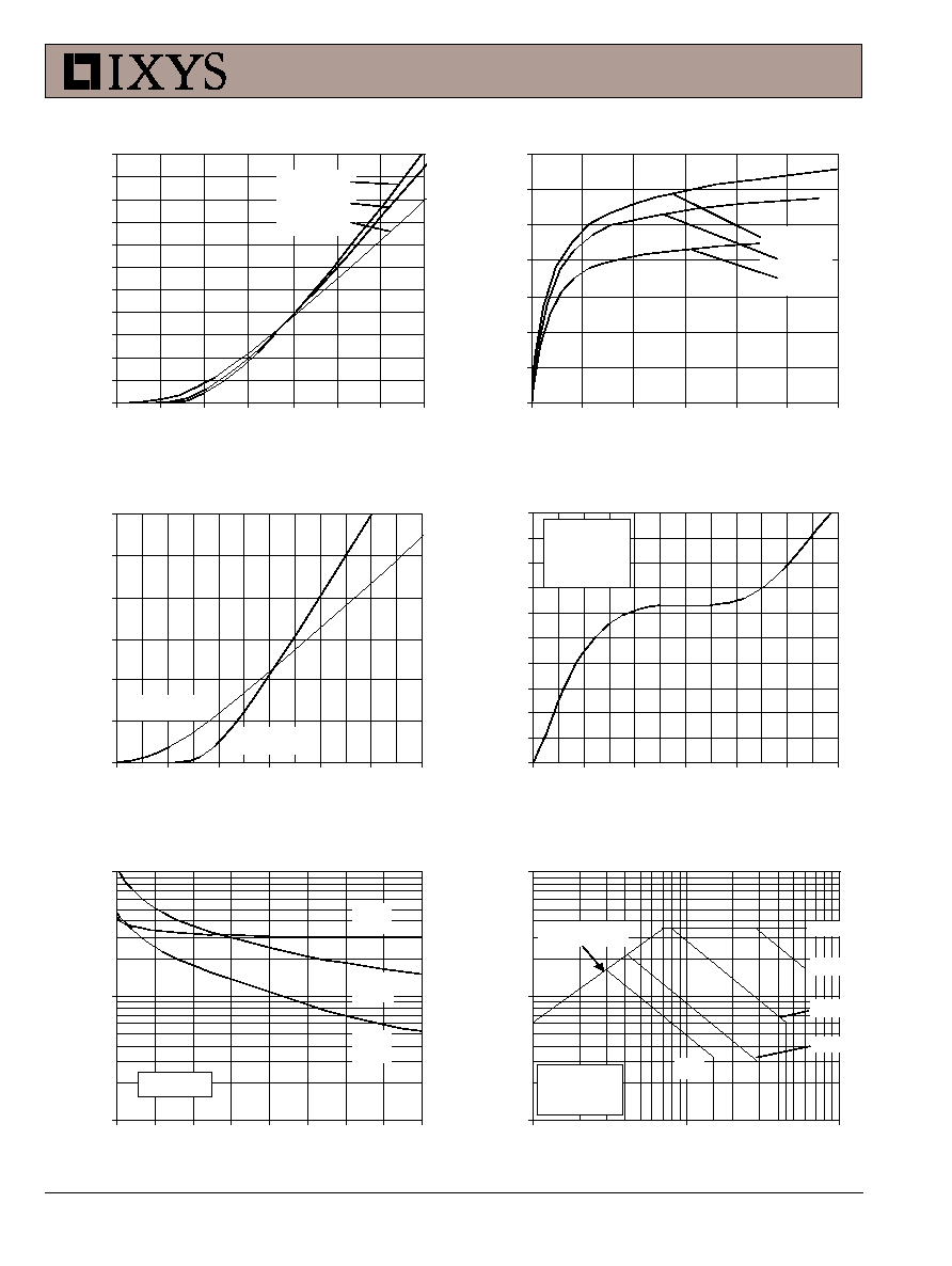
Fig. 4. R
DS(on
)
Norm alized to 0.5 I
D25
Value vs. Junction Tem perature
0.6
0.8
1
1.2
1.4
1.6
1.8
2
2.2
2.4
-50
-25
0
25
50
75
100
125
150
175
T
J
- Degrees Centigrade
R
D
S
(
o n )
-
N
o
r
m
a
liz
e
d
I
D
= 150A
I
D
= 75A
V
GS
= 10V
Fig. 6. Drain Current vs. Case
Tem perature
0
10
20
30
40
50
60
70
80
90
-50
-25
0
25
50
75
100
125 150
175
T
C
- Degrees Centigrade
I
D
-
A
m
p
e
re
s
External Lead Current Limit
Fig. 5. R
DS(on)
Norm alized to 0.5 I
D25
Value vs. Drain Current
0.6
0.8
1
1.2
1.4
1.6
1.8
2
2.2
2.4
2.6
2.8
0
25
50
75
100 125 150 175 200 225 250
I
D
- Amperes
R
D
S
(
o n )
-
N
o
r
m
a
liz
e
d
T
J
= 25
∫
C
V
GS
= 10V
T
J
= 175
∫
C
V
GS
= 15V
IXYS reserves the right to change limits, test conditions, and dimensions.
IXTQ 150N06P
IXYS MOSFETs and IGBTs are covered by one or more
4,850,072
4,931,844
5,034,796
5,063,307
5,237,481
5,381,025
6,404,065B1 6,162,665
6,534,343
6,583,505
of the following U.S. patents:
4,835,592
4,881,106
5,017,508
5,049,961
5,187,117
5,486,715
6,306,728B1
6,259,123B1 6,306,728B1 6,683,344
Fig. 11. Capacitance
100
1000
10000
0
5
10
15
20
25
30
35
40
V
DS
- Volts
C
a
pa
c
i
t
a
nc
e -
pi
c
o
F
a
r
a
d
s
Ciss
Coss
Crss
f = 1MHz
Fig. 10. Gate Charge
0
1
2
3
4
5
6
7
8
9
10
0
20
40
60
80
100
120
Q
G
- nanoCoulombs
V
G S
- V
o
l
t
s
V
DS
= 30V
I
D
= 75A
I
G
= 10mA
Fig. 7. Input Adm ittance
0
25
50
75
100
125
150
175
200
225
250
275
3
4
5
6
7
8
9
10
V
G S
- Volts
I
D
- A
m
p
e
r
e
s
T
J
= -40
∫
C
25
∫
C
150
∫
C
Fig. 8. Transconductance
0
10
20
30
40
50
60
70
0
50
100
150
200
250
300
I
D
- Amperes
g
f s
-
S
i
em
en
s
T
J
= -40
∫
C
25
∫
C
150
∫
C
Fig. 9. Source Current vs.
Source-To-Drain Voltage
0
50
100
150
200
250
300
0.4
0.6
0.8
1
1.2
1.4
1.6
V
S D
- Volts
I
S
- A
m
p
e
re
s
T
J
= 150
∫
C
T
J
= 25
∫
C
Fig. 12. Forw ard-Bias
Safe Operating Area
10
100
1000
1
10
100
V
D S
- Volts
I
D
- A
m
p
e
re
s
100µs
1ms
DC
T
J
= 175
∫
C
T
C
= 25
∫
C
R
DS(on)
Limit
10ms
25µs

© 2004 IXYS All rights reserved
IXTQ 150N06P
F ig . 1 3 . M a x im u m T r a n s ie n t T h e r m a l R e s is t a n c e
0 . 0 1
0 . 1 0
1 . 0 0
0 . 1
1
1 0
1 0 0
1 0 0 0
Pu ls e W id th - m illis e c o n d s
R
( t h ) J
C
-
∫C
/ W