
© 2005 IXYS All rights reserved
G = Gate
D = Drain
S = Source
TAB = Drain
DS99251B(02/05)
PolarHV
TM
Power MOSFET
V
DSS
= 600
V
I
D25
= 30
A
R
DS(on)
240 m
Advanced Technical Information
N-Channel Enhancement Mode
Fast Recovery Diode
Avalanche Rated
Features
Fast Recovery diode
Unclamped Inductive Switching (UIS)
rated
International standard packages
Low package inductance
- easy to drive and to protect
TO-3P (IXTQ)
Symbol
Test Conditions
Maximum Ratings
V
DSS
T
J
= 25
∞C to 150∞C
600
V
V
DGR
T
J
= 25
∞C to 150∞C; R
GS
= 1 M
600
V
V
GSS
Continuous
±30
V
V
GSM
Transient
±40
V
I
D25
T
C
= 25
∞C
30
A
I
DM
T
C
= 25
∞C, pulse width limited by T
JM
80
A
I
AR
T
C
= 25
∞C
30
A
E
AR
T
C
= 25
∞C
50
mJ
E
AS
T
C
= 25
∞C
1.5
J
dv/dt
I
S
I
DM
, di/dt
100 A/µs, V
DD
V
DSS
,
10
V/ns
T
J
150∞C, R
G
= 4
P
D
T
C
= 25
∞C
500
W
T
J
-55 ... +150
∞C
T
JM
150
∞C
T
stg
-55 ... +150
∞C
T
L
1.6 mm (0.062 in.) from case for 10 seconds
300
∞C
Plastic body FOR 10 seconds
260
∞C
M
d
Mounting torque
(TO-3P)
1.13/10 Nm/lb.in.
Weight
TO-247
6.0
g
TO-3P
5.5
g
PLUS220
4.0
g
TO-268
5.0
g
IXTH 30N60P
IXTQ 30N60P
IXTT 30N60P
IXTV 30N60P
IXTV 30N60PS
TO-268 (IXTT)
G
S
D (TAB)
PLUS220 (IXFV)
TO-247 (IXFH)
G
D
S
D (TAB)
Symbol
Test Conditions
Characteristic Values
(T
J
= 25
∞C, unless otherwise specified)
Min. Typ.
Max.
V
DSS
V
GS
= 0 V, I
D
= 250
µA
600
V
V
GS(th)
V
DS
= V
GS
, I
D
= 250
µA
2.5
5.0
V
I
GSS
V
GS
=
±30 V, V
DS
= 0
±100
nA
I
DSS
V
DS
= V
DSS
25
µA
V
GS
= 0 V
T
J
= 125
∞C
250
µA
R
DS(on)
V
GS
= 10 V, I
D
= 0.5 I
D25
240
m
Pulse test, t
300 µs, duty cycle d 2 %
G
D
S
D (TAB)
PLUS220 (IXFV...S)
G
S
D
D (TAB)
G
S
D (TAB)

IXYS reserves the right to change limits, test conditions, and dimensions.
IXTH 30N60P IXTQ 30N60P
IXTT 30N60P IXTV 30N60P
Fig. 2. Extended Output Characteristics
@ 25
∫
C
0
5
10
15
20
25
30
35
40
45
50
55
60
0
3
6
9
12
15
18
21
24
27
30
V
D S
- Volts
I
D
-
A
m
per
es
V
GS
= 10V
8V
7V
5V
6.5V
6V
5.5V
Fig. 1. Output Characteristics
@ 25
∫
C
0
3
6
9
12
15
18
21
24
27
30
0
1
2
3
4
5
6
7
8
V
D S
- Volts
I
D
- A
m
p
e
r
e
s
V
GS
= 10V
8V
7V
5.5V
5V
6.5V
6V
IXYS MOSFETs and IGBTs are covered by
4,835,592
4,931,844
5,049,961
5,237,481
6,162,665
6,404,065 B1
6,683,344
6,727,585
one or moreof the following U.S. patents:
4,850,072
5,017,508
5,063,307
5,381,025
6,259,123 B1
6,534,343
6,710,405B2
6,759,692
4,881,106
5,034,796
5,187,117
5,486,715
6,306,728 B1
6,583,505
6,710,463
Symbol
Test Conditions
Characteristic Values
(T
J
= 25
∞C, unless otherwise specified)
Min.
Typ. Max.
g
fs
V
DS
= 20 V; I
D
= 0.5 I
D25
, pulse test
22
25
S
C
iss
5050
pF
C
oss
V
GS
= 0 V, V
DS
= 25 V, f = 1 MHz
540
pF
C
rss
53
pF
t
d(on)
29
ns
t
r
V
GS
= 10 V, V
DS
= 0.5 I
D25
20
ns
t
d(off)
R
G
= 4
(External)
80
ns
t
f
25
ns
Q
g(on)
82
nC
Q
gs
V
GS
= 10 V, V
DS
= 0.5 V
DSS
, I
D
= 0.5 I
D25
28
nC
Q
gd
30
nC
R
thJC
0.19 K/W
R
thCK
0.21
K/W
Source-Drain Diode
Characteristic Values
(T
J
= 25
∞C, unless otherwise specified)
Symbol
Test Conditions
min.
typ. max.
I
S
V
GS
= 0 V
30
A
I
SM
Repetitive
80
A
V
SD
I
F
= I
S
, V
GS
= 0 V,
1.5
V
Pulse test, t
300 µs, duty cycle d 2 %
t
rr
I
F
= 25A, -di/dt = 100 A/
µs
410
ns
Q
RM
V
R
= 100V
4.0
µC

© 2005 IXYS All rights reserved
IXTH 30N60P IXTQ 30N60P
IXTT 30N60P IXTV 30N60P
Fig. 3. Output Characteristics
@ 125
∫
C
0
3
6
9
12
15
18
21
24
27
30
0
2
4
6
8
10
12
14
16
18
V
D S
- Volts
I
D
- A
m
p
e
r
e
s
V
GS
= 10V
7V
5.5V
5V
4.5V
6V
Fig. 4. R
DS(on
)
Norm alized to 0.5 I
D25
Value vs. Junction Tem perature
0.4
0.7
1
1.3
1.6
1.9
2.2
2.5
2.8
3.1
3.4
-50
-25
0
25
50
75
100
125
150
T
J
- Degrees Centigrade
R
D S
(
o
n
)
- N
o
rm
a
l
i
z
e
d
I
D
= 30A
I
D
= 15A
V
GS
= 10V
Fig. 6. Drain Current vs. Case
Tem perature
0
5
10
15
20
25
30
35
-50
-25
0
25
50
75
100
125
150
T
C
- Degrees Centigrade
I
D
-
A
m
p
e
re
s
Fig. 5. R
DS(on)
Norm alized to
0.5 I
D25
Value vs. I
D
0.8
1
1.2
1.4
1.6
1.8
2
2.2
2.4
2.6
2.8
3
0
5
10 15 20 25
30 35 40 45
50 55 60
I
D
- Amperes
R
D S
(
o
n
)
- N
o
rm
a
l
i
z
e
d
T
J
= 125
C
T
J
= 25
C
V
GS
= 10V
Fig. 7. Input Admittance
0
5
10
15
20
25
30
35
3.5
4
4.5
5
5.5
6
6.5
7
V
G S
- Volts
I
D
- A
m
p
e
r
e
s
T
J
= 125
C
25
C
-40
C
Fig. 8. Transconductance
0
5
10
15
20
25
30
35
40
45
50
0
5
10
15
20
25
30
35
40
I
D
- Amperes
g
f s
-
S
i
em
en
s
T
J
= -40
C
25
C
125
C
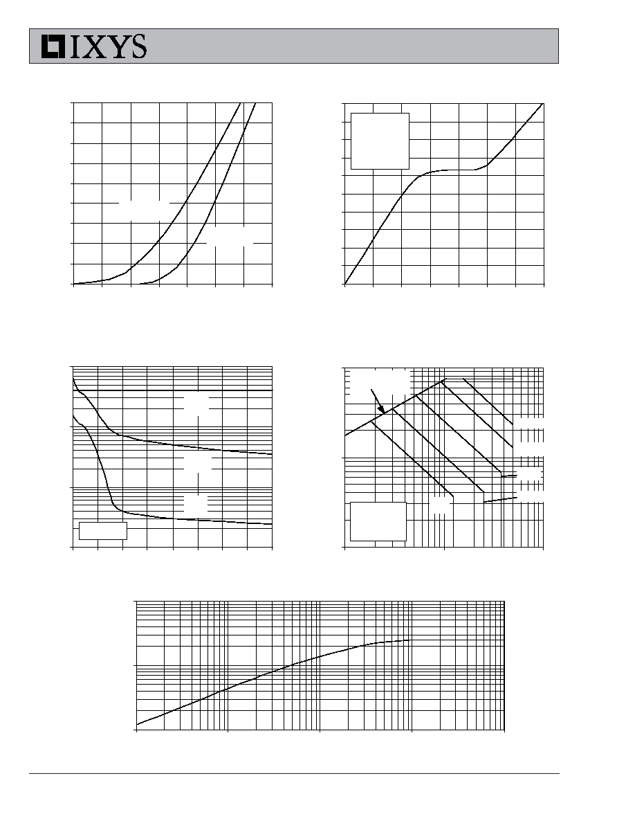
IXYS reserves the right to change limits, test conditions, and dimensions.
IXTH 30N60P IXTQ 30N60P
IXTT 30N60P IXTV 30N60P
Fig. 13. Maximum Transient Thermal Resistance
0.01
0.10
1.00
0.1
1
10
100
1000
Pulse Width - milliseconds
R
( t h
) J
C
-
C /
W
Fig. 11. Capacitance
10
100
1000
10000
0
5
10
15
20
25
30
35
40
V
D S
- Volts
C
a
pac
i
t
a
n
c
e
-
p
i
c
o
F
a
r
a
ds
Ciss
Coss
Crs
f = 1MHz
Fig. 10. Gate Charge
0
1
2
3
4
5
6
7
8
9
10
0
10
20
30
40
50
60
70
Q
G
- nanoCoulombs
V
G S
- V
o
l
t
s
V
DS
= 250V
I
D
= 15A
I
G
= 10mA
Fig. 9. Source Current vs.
Source-To-Drain Voltage
0
10
20
30
40
50
60
70
80
90
0.4
0.5
0.6
0.7
0.8
0.9
1
1.1
V
S D
- Volts
I
S
- A
m
p
e
r
e
s
T
J
= 125
C
T
J
= 25
C
Fig. 12. Forw ard-Bias
Safe Operating Area
1
10
100
10
100
1000
V
D S
- Volts
I
D
-
A
m
per
es
100µs
1ms
DC
T
J
= 150C
T
C
= 25C
R
DS(on)
Limit
10ms
25µs

© 2005 IXYS All rights reserved
IXTH 30N60P IXTQ 30N60P
IXTT 30N60P IXTV 30N60P
Package Outline Drawings
D1
L
L3
L1
E1
e
E
b
D
c
A2
A1
A
L2
Terminals: 1 - Gate
2 - Drain
3 - Source
TAB - Drain
E1
E
L2
D
L3
L
L1
3X b
2X e
c
A2
A1
A
E1
D1
PLUS220 (IXTV) Outline
TO-247AD (IXTH) Outline
Terminals: 1 - Gate
2 - Drain
3 - Source
Tab - Drain
1 2 3
TO-3P (IXTQ) Outline
TO-268 (IXTT) Outline
Dim.
Millimeter
Inches
Min.
Max.
Min.
Max.
A
4.7
5.3
.185
.209
A
1
2.2
2.54
.087
.102
A
2
2.2
2.6
.059
.098
b
1.0
1.4
.040
.055
b
1
1.65
2.13
.065
.084
b
2
2.87
3.12
.113
.123
C
.4
.8
.016
.031
D
20.80
21.46
.819
.845
E
15.75
16.26
.610
.640
e
5.20
5.72
0.205 0.225
L
19.81
20.32
.780
.800
L1
4.50
.177
P
3.55
3.65
.140
.144
Q
5.89
6.40
0.232 0.252
R
4.32
5.49
.170
.216
S
6.15 BSC
242 BSC

IXYS reserves the right to change limits, test conditions, and dimensions.
IXTH 30N60P IXTQ 30N60P
IXTT 30N60P IXTV 30N60P
Package Outline Drawings
L
L3
L2
L1
A1
E1
e
D1
E
b
D
c
A2
A
A3
L4
Terminals: 1-Gate 2-Drain
E
E1
D
L2
A
A1
L1
L
L3
e
2X b
c
A2
L4
A3
E1
PLUS220SMD (IXTV..S) Outline