
© 2005 IXYS All rights reserved
Symbol
Test Conditions
Maximum Ratings
V
DSS
T
J
= 25
∞C to 150∞C
500
V
V
DGR
T
J
= 25
∞C to 150∞C; R
GS
= 1 M
500
V
V
GSS
Continuous
±30
V
V
GSM
Transient
±40
V
I
D25
T
C
= 25
∞C
30
A
I
DM
T
C
= 25
∞C, pulse width limited by T
JM
75
A
I
AR
T
C
= 25
∞C
30
A
E
AR
T
C
= 25
∞C
40
mJ
E
AS
T
C
= 25
∞C
1.2
J
dv/dt
I
S
I
DM
, di/dt
100 A/µs, V
DD
V
DSS
,
10
V/ns
T
J
150∞C, R
G
= 5
P
D
T
C
= 25
∞C
460
W
T
J
-55 ... +150
∞C
T
JM
150
∞C
T
stg
-55 ... +150
∞C
T
L
1.6 mm (0.062 in.) from case for 10 s
300
∞C
Maximum tab temperature for soldering
260
∞C
for 10s
M
d
Mounting torque (TO-247, TO-3P)
1.13/10 Nm/lb.in.
Weight
TO-247
6
g
TO-268
5 g
PLUS220, PLUS220SMD
4
g
TO-3P 5.5 g
G = Gate
D = Drain
S = Source
TAB = Drain
DS99415(07/05)
PolarHV
TM
Power
MOSFET
Advance Technical Information
N-Channel Enhancement
ModeAvalanche Rated
Features
International standard packages
Unclamped Inductive Switching (UIS)
rated
Low package inductance
- easy to drive and to protect
IXTH 30N50P
IXTT 30N50P
IXTQ 30N50P
IXTV 30N50P
IXTV 30N50PS
V
DSS
= 500 V
I
D25
= 30 A
R
DS(on)
= 200 m
TO-247 AD (IXTH)
(TAB)
TO-268 (IXTT)
G
S
D (TAB)
G
S
D
PLUS220 (IXTV)
TO-3P (IXTQ)
G
D
S
(TAB)
Symbol
Test Conditions
Characteristic Values
(T
J
= 25
∞C, unless otherwise specified) Min. Typ. Max.
V
DSS
V
GS
= 0 V, I
D
= 250
µA
500
V
V
GS(th)
V
DS
= V
GS
, I
D
= 250
µA
3.0
5.0
V
I
GSS
V
GS
=
±30 V
DC
, V
DS
= 0
±100
nA
I
DSS
V
DS
= V
DSS
25
µA
V
GS
= 0 V
T
J
= 125
∞C
250
µA
R
DS(on)
V
GS
= 10 V, I
D
= 0.5 I
D25
165
200
m
Pulse test, t
300 µs, duty cycle d 2 %
PLUS220 SMD(IXTV..S)
D (TAB)
D (TAB)
G
S

IXYS reserves the right to change limits, test conditions, and dimensions.
IXTH 30N50P IXTQ 30N50P IXTT 30N50P
IXTV 30N50P IXTV 30N50PS
IXYS MOSFETs and IGBTs are covered by
4,835,592
4,931,844
5,049,961
5,237,481
6,162,665
6,404,065 B1
6,683,344
6,727,585
one or moreof the following U.S. patents:
4,850,072
5,017,508
5,063,307
5,381,025
6,259,123 B1
6,534,343
6,710,405B2
6,759,692
4,881,106
5,034,796
5,187,117
5,486,715
6,306,728 B1
6,583,505
6,710,463
Symbol
Test Conditions Characteristic Values
(T
J
= 25
∞C, unless otherwise specified)
Min.
Typ.
Max.
g
fs
V
DS
= 20 V; I
D
= 0.5 I
D25
, pulse test
17
27
S
C
iss
4150
pF
C
oss
V
GS
= 0 V, V
DS
= 25 V, f = 1 MHz
445
pF
C
rss
28
pF
t
d(on)
25
n s
t
r
V
GS
= 10 V, V
DS
= 0.5 V
DSS
, I
D
= I
D25
27
n s
t
d(off)
R
G
= 5
(External)
75
ns
t
f
21
n s
Q
g(on)
70
nC
Q
gs
V
GS
= 10 V, V
DS
= 0.5 V
DSS
, I
D
= 0.5 I
D25
27
nC
Q
gd
22
nC
R
thJC
0.27 K/W
R
thCK
(TO-247, TO-3P and PLUS220)
0.21
K/W
Source-Drain Diode Characteristic Values
(T
J
= 25
∞C, unless otherwise specified)
Symbol
Test Conditions
Min.
typ.
Max.
I
S
V
GS
= 0 V
30
A
I
SM
Repetitive
90
A
V
SD
I
F
= I
S
, V
GS
= 0 V,
1.5
V
Pulse test, t
300 µs, duty cycle d 2 %
t
rr
I
F
= 18 A, -di/dt = 100 A/
µs
400
ns
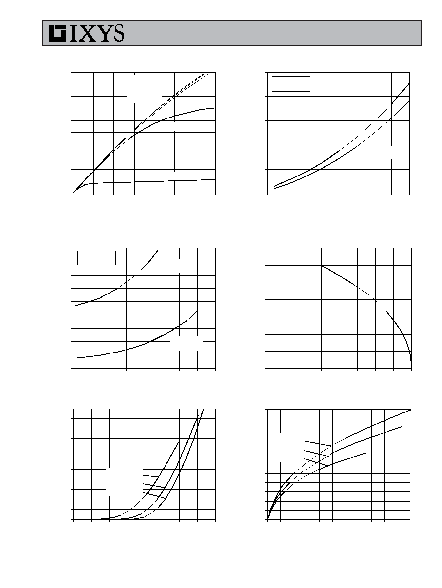
Fig. 2. Extended Output Characteristics
@ 25
∫
C
0
10
20
30
40
50
60
70
0
3
6
9
12
15
18
21
24
27
30
V
D S
- Volts
I
D
-
A
m
per
es
V
GS
= 10V
8V
7V
6V
Fig. 1. Output Characteristics
@ 25
∫
C
0
3
6
9
12
15
18
21
24
27
30
0
1
2
3
4
5
6
7
V
D S
- Volts
I
D
- A
m
p
e
r
e
s
V
GS
= 10V
8V
7V
6V
© 2005 IXYS All rights reserved
Fig. 3. Output Characteristics
@ 125
∫
C
0
3
6
9
12
15
18
21
24
27
30
0
2
4
6
8
10
12
14
V
D S
- Volts
I
D
- A
m
p
e
r
e
s
V
GS
= 10V
8V
7V
5V
6V
Fig. 4. R
DS(on
)
Norm alized to 0.5 I
D25
Value vs. Junction Tem perature
0.4
0.7
1
1.3
1.6
1.9
2.2
2.5
2.8
3.1
3.4
-50
-25
0
25
50
75
100
125
150
T
J
- Degrees Centigrade
R
D S
(
o
n
)
-
N
o
r
m
al
i
z
ed
I
D
= 30A
I
D
= 15A
V
GS
= 10V
Fig. 6. Drain Current vs. Case
Tem perature
0
5
10
15
20
25
30
35
-50
-25
0
25
50
75
100
125
150
T
C
- Degrees Centigrade
I
D
- A
m
p
e
re
s
Fig. 5. R
DS(on)
Norm alized to
0.5 I
D25
Value vs. I
D
0.7
1
1.3
1.6
1.9
2.2
2.5
2.8
3.1
3.4
0
10
20
30
40
50
60
70
80
I
D
- Amperes
R
D S
(
o
n
)
-
N
o
rm
a
l
i
z
e
d
T
J
= 125
C
T
J
= 25
C
V
GS
= 10V
Fig. 7. Input Adm ittance
0
5
10
15
20
25
30
35
40
45
50
55
3.5
4
4.5
5
5.5
6
6.5
7
7.5
V
G S
- Volts
I
D
-
A
m
per
es
T
J
= 125
C
25
C
-40
C
Fig. 8. Transconductance
0
5
10
15
20
25
30
35
40
45
50
55
60
0
5
10
15
20
25
30
35
40
45
50
55
I
D
- Amperes
g
f s
-
S
i
em
ens
T
J
= -40
C
25
C
125
C
IXTH 30N50P IXTQ 30N50P IXTT 30N50P
IXTV 30N50P IXTV 30N50PS
IXYS reserves the right to change limits, test conditions, and dimensions.
IXTH 30N50P IXTQ 30N50P IXTT 30N50P
IXTV 30N50P IXTV 30N50PS
IXYS MOSFETs and IGBTs are covered by
4,835,592
4,931,844
5,049,961
5,237,481
6,162,665
6,404,065 B1
6,683,344
6,727,585
one or moreof the following U.S. patents:
4,850,072
5,017,508
5,063,307
5,381,025
6,259,123 B1
6,534,343
6,710,405B2
6,759,692
4,881,106
5,034,796
5,187,117
5,486,715
6,306,728 B1
6,583,505
6,710,463
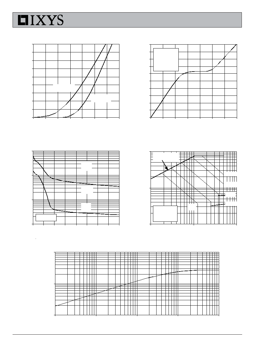
Fig. 11. Capacitance
10
100
1000
10000
0
5
10
15
20
25
30
35
40
V
D S
- Volts
C
a
p
a
c
i
t
a
nc
e -
p
i
c
o
F
a
r
a
ds
Ciss
Coss
Crs
f = 1MHz
Fig. 10. Gate Charge
0
1
2
3
4
5
6
7
8
9
10
0
10
20
30
40
50
60
70
Q
G
- nanoCoulombs
V
G S
- V
o
l
t
s
V
DS
= 250V
I
D
= 15A
I
G
= 10mA
Fig. 9. Source Current vs.
Source-To-Drain Voltage
0
10
20
30
40
50
60
70
80
90
0.4
0.5
0.6
0.7
0.8
0.9
1
1.1
V
S D
- Volts
I
S
- A
m
p
e
re
s
T
J
= 125
C
T
J
= 25
C
Fig. 12. Forw ard-Bias
Safe Operating Area
1
10
100
10
100
1000
V
D S
- Volts
I
D
- A
m
p
e
re
s
100µs
1ms
DC
T
J
= 150C
T
C
= 25C
R
DS(on)
Limit
10ms
25µs
Fig. 13. M axim um Trans ie nt The r m al Re s is tance
0.01
0.10
1.00
0.1
1
10
100
1000
Pulse Width - millisec onds
R
( t
h
) J
C
-
C / W

© 2005 IXYS All rights reserved
TO-247 AD (IXTH) Outline
Terminals:
1 - Gate
2 - Drain
3 - Source
Tab - Drain
1 2 3
Dim.
Millimeter
Inches
Min.
Max.
Min.
Max.
A
4.7
5.3
.185
.209
A
1
2.2
2.54
.087
.102
A
2
2.2
2.6
.059
.098
b
1.0
1.4
.040
.055
b
1
1.65
2.13
.065
.084
b
2
2.87
3.12
.113
.123
C
.4
.8
.016
.031
D
20.80
21.46
.819
.845
E
15.75
16.26
.610
.640
e
5.20
5.72
0.205
0.225
L
19.81
20.32
.780
.800
L1
4.50
.177
P
3.55
3.65
.140
.144
Q
5.89
6.40
0.232
0.252
R
4.32
5.49
.170
.216
S
6.15
BSC
242
BSC
D1
L
L3
L1
E1
e
E
b
D
c
A2
A1
A
L2
Terminals: 1-Gate 2-Drain
E1
E
L2
D
L3
L
L1
3X b
2X e
c
A2
A1
A
E1
D1
PLUS220 (IXTV) Outline
TO-3P (IXTQ) Outline
L
L3
L2
L1
A1
E1
e
D1
E
b
D
c
A2
A
A3
L4
Terminals: 1-Gate 2-Drain
E
E1
D
L2
A
A1
L1
L
L3
e
2X b
c
A2
L4
A3
E1
Package Outline Drawings
TO-268 (IXTT) Outline
IXTH 30N50P IXTQ 30N50P IXTT 30N50P
IXTV 30N50P IXTV 30N50PS