
© 1997 IXYS All rights reserved
S
G
S
D
G = Gate
D = Drain
S = Source
Either Source terminal at miniBLOC can be used
as Main or Kelvin Source
High Current
Power MOSFET
N-Channel Enhancement Mode
V
DSS
I
D25
R
DS(on)
IXTN 58N50
500 V
58 A 85
m
IXTN 61N50
500 V
61 A 75 m
Symbol
Test Conditions
Maximum Ratings
V
DSS
T
J
= 25∞C to 150∞C
500
V
V
DGR
T
J
= 25∞C to 150∞C; R
GS
= 1.0 M
500
V
V
G S
Continuous
±
20
V
V
GSM
Transient
±
30
V
I
D25
T
C
= 25∞C
IXTN 58N50
58
A
IXTN 61N50
61
A
I
DM
T
C
= 25∞C
IXTN 58N50
232
A
Pulse width limited by T
JM
IXTN 61N50
244
A
P
D
T
C
= 25∞C
625
W
T
J
-40 ... +150
∞C
T
JM
150
∞C
T
stg
-40 ... +150
∞C
V
ISOL
50/60 Hz, RMS
t = 1 minute
2500
V~
t = 1s
3000
V~
M
d
Mounting torque
1.5/13 Nm/lb.in.
Terminal connection torque (M4)
1.5/13 Nm/lb.in.
Weight
30
g
Symbol
Test Conditions
Characteristic Values
(T
J
= 25∞C unless otherwise specified)
Min. Typ.
Max.
V
DSS
V
GS
= 0 V, I
D
= 5 mA
500
V
V
GS(th)
V
DS
= V
GS
,
I
D
= 12 mA
1.7
4.0
V
I
GSS
V
GS
=
±
20 V DC, V
DS
= 0
±
200
nA
I
DSS
V
DS
= 0.8 V
DSS
T
J
= 25∞C
500
µA
V
GS
= 0 V
T
J
= 125∞C
2
mA
R
DS(on)
V
GS
= 10 V, I
D
= 0.5 I
D25
58N50
85
m
61N50
75
m
Pulse test, t
300 µs, duty cycle
2 %
Preliminary Data
Features
∑ International standard package
∑ Isolation voltage 3000V (RMS)
∑ Low R
DS (on)
HDMOS
TM
process
∑ Rugged polysilicon gate cell structure
∑ Low drain-to-case capacitance
(<100 pF)
- reduced RFI
∑ Low package inductance (< 10 nH)
- easy to drive and to protect
∑ Aluminium Nitride Isolation
- increased current ratings
Applications
∑ DC choppers
∑ AC motor speed controls
∑ DC servo and robot drives
∑ Uninterruptible power supplies (UPS)
∑ Switched mode and resonant mode
power supplies
Advantages
∑ Easy to mount
∑ Space savings
∑ High power density
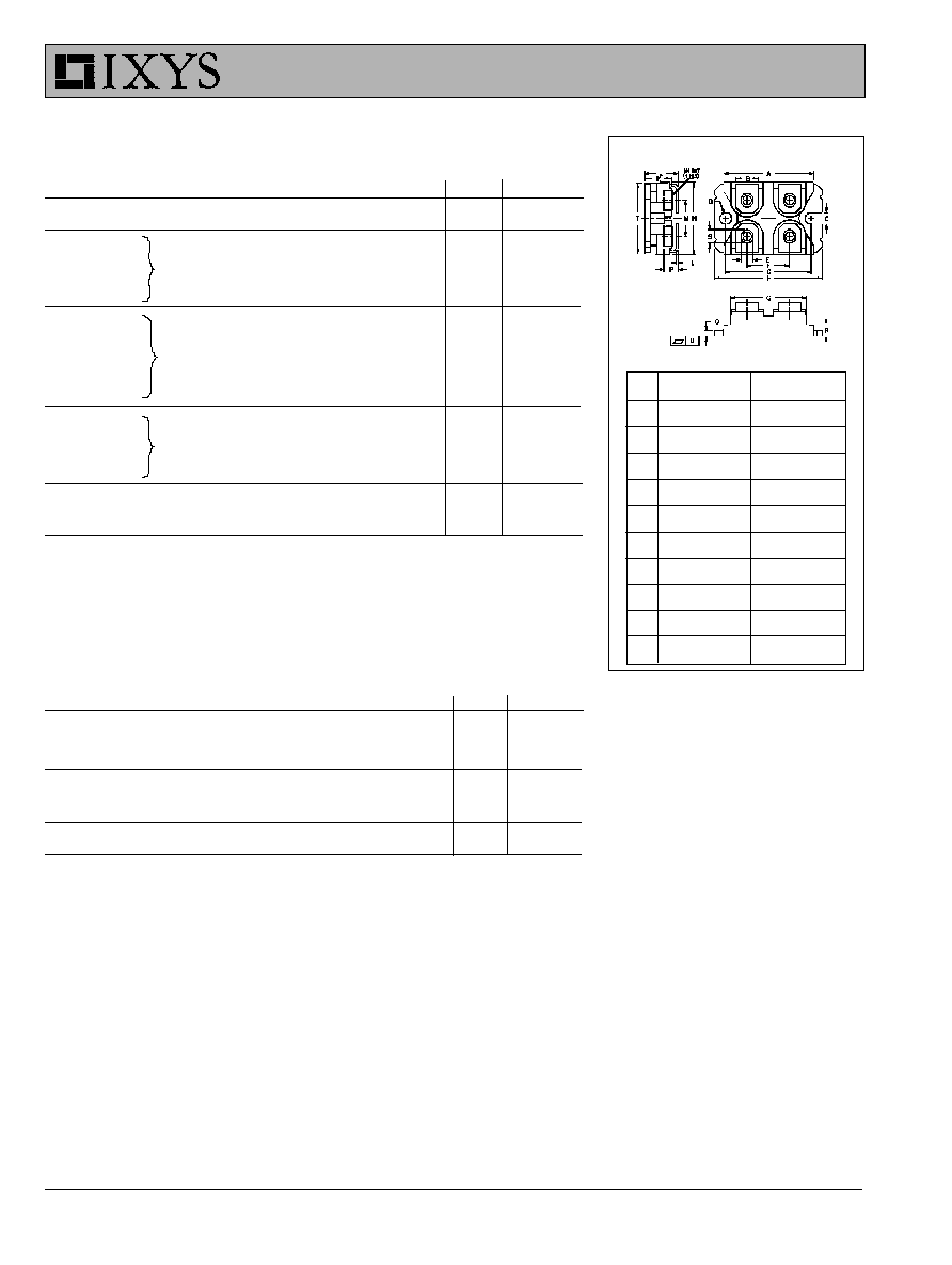
miniBLOC, SOT-227 B
E153432
95501B(4/97)
IXYS MOSFETS and IGBTs are covered by one or more of the following U.S. patents:
4,835,592
4,881,106
5,017,508
5,049,961
5,187,117
5,486,715
4,850,072
4,931,844
5,034,796
5,063,307
5,237,481
5,381,025
IXYS reserves the right to change limits, test conditions, and dimensions.
IXTN 58N50
IXTN 61N50
Symbol
Test Conditions
Characteristic Values
(T
J
= 25∞C unless otherwise specified)
Min. Typ.
Max.
g
fs
V
DS
= 10 V; I
D
= 0.5 I
D25
, pulse test
20
30
S
C
iss
11000
pF
C
oss
V
GS
= 0 V, V
DS
= 25 V, f = 1 MHz
1550
pF
C
rss
225
pF
t
d(on)
30
ns
t
r
V
GS
= 10 V, V
DS
= 0.5 V
DSS
, I
D
= 50 A
60
ns
t
d(off)
R
G
= 1
(External)
100
ns
t
f
50
ns
Q
g
420
nC
Q
gs
V
GS
= 10 V, V
DS
= 0.5 V
DSS
, I
D
= I
D2
55
nC
Q
gd
160
nC
R
thJC
0.20 K/W
R
thCK
0.05
K/W
Source-Drain Diode
Ratings and Characteristics
(T
J
= 25∞C unless otherwise specified)
Symbol
Test Conditions
Min. Typ. Max.
I
S
V
GS
= 0 V
61
A
I
SM
Repetitive; pulse width limited by T
JM
244
A
V
SD
I
F
= I
S,
V
GS
= 0 V,
1.5
V
Pulse test, t
300 µs, duty cycle
2 %
t
rr
I
F
= 50A
,
di/dt = -100 A/µs, V
R
= 100 V
800
ns
miniBLOC, SOT-227 B
M4 screws (4x) supplied
Dim.
Millimeter
Inches
Min.
Max.
Min.
Max.
A
31.50
31.88
1.240
1.255
B
7.80
8.20
0.307
0.323
C
4.09
4.29
0.161
0.169
D
4.09
4.29
0.161
0.169
E
4.09
4.29
0.161
0.169
F
14.91
15.11
0.587
0.595
G
30.12
30.30
1.186
1.193
H
38.00
38.23
1.496
1.505
J
11.68
12.22
0.460
0.481
K
8.92
9.60
0.351
0.378
L
0.76
0.84
0.030
0.033
M
12.60
12.85
0.496
0.506
N
25.15
25.42
0.990
1.001
O
1.98
2.13
0.078
0.084
P
4.95
5.97
0.195
0.235
Q
26.54
26.90
1.045
1.059
R
3.94
4.42
0.155
0.174
S
4.72
4.85
0.186
0.191
T
24.59
25.07
0.968
0.987
U
-0.05
0.1
-0.002
0.004