
© 2005 IXYS All rights reserved
Symbol
Test Conditions
Maximum Ratings
V
DSS
T
J
= 25
∞C to 150∞C
500
V
V
DGR
T
J
= 25
∞C to 150∞C; R
GS
= 1 M
500
V
V
GSM
±30
V
I
D25
T
C
= 25
∞C
22
A
I
DM
T
C
= 25
∞C, pulse width limited by T
JM
66
A
I
AR
T
C
= 25
∞C
22
A
E
AR
T
C
= 25
∞C
30
mJ
E
AS
T
C
= 25
∞C
750
mJ
dv/dt
I
S
I
DM
, di/dt
100 A/µs, V
DD
V
DSS
,
10
V/ns
T
J
150∞C, R
G
= 10
P
D
T
C
= 25
∞C
350
W
T
J
-55 ... +150
∞C
T
JM
150
∞C
T
stg
-55 ... +150
∞C
T
L
1.6 mm (0.062 in.) from case for 10 s
300
∞C
Maximum tab temperature for soldering
260
∞C
for 10s
M
d
Mounting torque
1.13/10 Nm/lb.in.
Weight
TO-3P
5.5
g
PLUS220 & PLUS220SMD
4
g
DS99351A(03/05)
Symbol
Test Conditions
Characteristic Values
(T
J
= 25
∞C, unless otherwise specified)
Min. Typ.
Max.
V
DSS
V
GS
= 0 V, I
D
= 250
µA
500
V
V
GS(th)
V
DS
= V
GS
, I
D
= 250
µA
3.0
5.0
V
I
GSS
V
GS
=
±20 V
DC
, V
DS
= 0
±10
nA
I
DSS
V
DS
= V
DSS
5
µA
V
GS
= 0 V
T
J
= 125
∞C
50
µA
R
DS(on)
V
GS
= 10 V, I
D
= 0.5 I
D25
270 m
Pulse test, t
300 µs, duty cycle d 2 %
PolarHV
TM
Power MOSFET
Advance Technical Information
N-Channel Enhancement Mode
Features
International standard packages
Unclamped Inductive Switching (UIS)
rated
Low package inductance
- easy to drive and to protect
Advantages
Easy to mount
Space savings
High power density
IXTQ 22N50P
IXTV 22N50P
IXTV 22N50PS
V
DSS
= 500 V
I
D25
= 22 A
R
DS(on)
= 270 m
TO-3P (IXTQ)
G
D
S
(TAB)
G = Gate
D = Drain
S = Source
TAB = Drain
G
S
D
PLUS220 (IXFV)
G
S
PLUS220SMD (IXFV-PS)
D (TAB)
D (TAB)
IXYS reserves the right to change limits, test conditions, and dimensions.
IXTQ 22N50P
IXTV 22N50PS IXTV 22N50P
IXYS MOSFETs and IGBTs are covered by
4,835,592
4,931,844
5,049,961
5,237,481
6,162,665
6,404,065 B1
6,683,344
6,727,585
one or moreof the following U.S. patents:
4,850,072
5,017,508
5,063,307
5,381,025
6,259,123 B1
6,534,343
6,710,405B2
6,759,692
4,881,106
5,034,796
5,187,117
5,486,715
6,306,728 B1
6,583,505
6,710,463
Symbol
Test Conditions Characteristic Values
(T
J
= 25
∞C, unless otherwise specified)
Min.
Typ.
Max.
g
fs
V
DS
= 20 V; I
D
= 0.5 I
D25
, pulse test
20
S
C
iss
3050
pF
C
oss
V
GS
= 0 V, V
DS
= 25 V, f = 1 MHz
340
pF
C
rss
40
pF
t
d(on)
25
n s
t
r
V
GS
= 10 V, V
DS
= 0.5 V
DSS
, I
D
= I
D25
27
n s
t
d(off)
R
G
= 18
(External)
75
n s
t
f
21
n s
Q
g(on)
70
nC
Q
gs
V
GS
= 10 V, V
DS
= 0.5 V
DSS
, I
D
= 0.5 I
D25
17
nC
Q
gd
40
nC
R
thJC
0.35 K/W
R
thCK
(TO-247)
0.21
K/W
R
thCK
(TO-3 P) 0.21 K/W
Source-Drain Diode Characteristic Values
(T
J
= 25
∞C, unless otherwise specified)
Symbol
Test Conditions
Min.
typ.
Max.
I
S
V
GS
= 0 V
16
A
I
SM
Repetitive
64
A
V
SD
I
F
= I
S
, V
GS
= 0 V,
1.5
V
Pulse test, t
300 µs, duty cycle d 2 %
t
rr
I
F
= 22 A
400
n s
-di/dt = 100 A/
µs
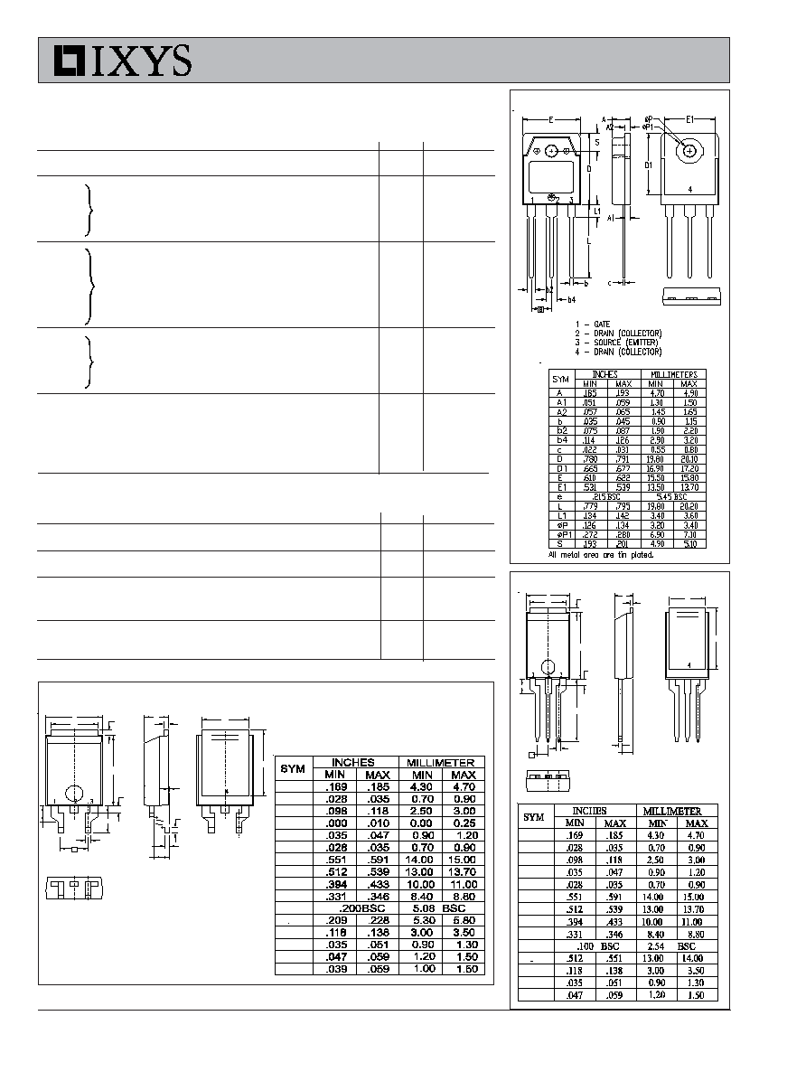
TO-3P (IXTQ) Outline
D1
L
L3
L1
E1
e
E
b
D
c
A2
A1
A
L2
E1
E
L2
D
L3
L
L1
3X b
2X e
c
A2
A1
A
E1
D1
PLUS220 (IXFV) Outline
Terminals: 1-Gate 2-Drain
L
L3
L2
L1
A1
E1
e
D1
E
b
D
c
A2
A
A3
L4
Terminals: 1-Gate 2-Drain
E
E1
D
L2
A
A1
L1
L
L3
e
2X b
c
A2
L4
A3
E1
PLUS220SMD (IXFV-PS) Outline

© 2005 IXYS All rights reserved
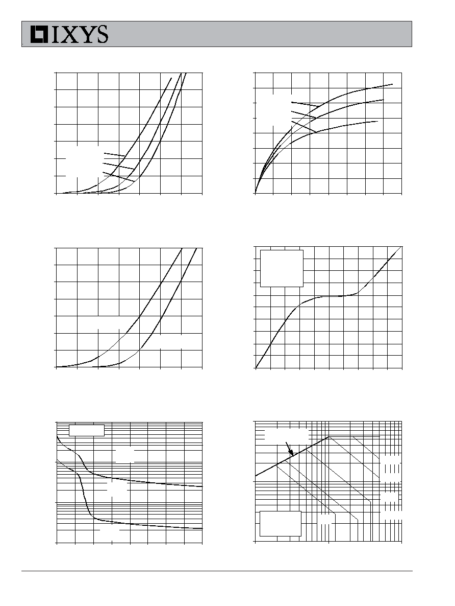
Fig. 2. Extended Output Characteristics
@ 25
∫
C
0
5
10
15
20
25
30
35
40
45
50
55
0
3
6
9
12
15
18
21
24
27
30
V
D S
- Volts
I
D
- A
m
p
e
re
s
V
GS
= 10V
8V
5V
7V
6V
Fig. 3. Output Characteristics
@ 125
∫
C
0
2
4
6
8
10
12
14
16
18
20
22
0
2
4
6
8
10
12
14
16
V
D S
- Volts
I
D
- A
m
p
e
r
e
s
V
GS
= 10V
7V
5V
6V
Fig. 1. Output Characteristics
@ 25
∫
C
0
2
4
6
8
10
12
14
16
18
20
22
0
1
2
3
4
5
6
7
V
D S
- Volts
I
D
- A
m
p
e
re
s
V
GS
= 10V
8V
7V
5V
6V
Fig. 4. R
DS(on
)
Normalized to 0.5 I
D25
Value vs. Junction Temperature
0.4
0.7
1
1.3
1.6
1.9
2.2
2.5
2.8
3.1
-50
-25
0
25
50
75
100
125
150
T
J
- Degrees Centigrade
R
D S
(
o
n
)
- N
o
rm
a
l
i
z
e
d
I
D
= 22A
I
D
= 11A
V
GS
= 10V
Fig. 6. Drain Current vs. Case
Tem perature
0
4
8
12
16
20
24
-50
-25
0
25
50
75
100
125
150
T
C
- Degrees Centigrade
I
D
-
A
m
per
es
Fig. 5. R
DS(on)
Normalized to
0.5 I
D25
Value vs. I
D
0.7
1
1.3
1.6
1.9
2.2
2.5
2.8
3.1
0
5
10
15
20
25
30
35
40
45
50
55
I
D
- Amperes
R
D
S
(
o n )
- N
o
rm
a
l
i
z
e
d
T
J
= 125
C
T
J
= 25
C
V
GS
= 10V
IXTQ 22N50P
IXTV 22N50PS IXTV 22N50P
IXYS reserves the right to change limits, test conditions, and dimensions.
IXTQ 22N50P
IXTV 22N50PS IXTV 22N50P
IXYS MOSFETs and IGBTs are covered by
4,835,592
4,931,844
5,049,961
5,237,481
6,162,665
6,404,065 B1
6,683,344
6,727,585
one or moreof the following U.S. patents:
4,850,072
5,017,508
5,063,307
5,381,025
6,259,123 B1
6,534,343
6,710,405B2
6,759,692
4,881,106
5,034,796
5,187,117
5,486,715
6,306,728 B1
6,583,505
6,710,463
Fig. 11. Capacitance
10
100
1000
10000
0
5
10
15
20
25
30
35
40
V
D S
- Volts
C
apac
i
t
anc
e -
pi
c
o
F
a
r
ads
Ciss
Coss
Crss
f = 1MHz
Fig. 10. Gate Charge
0
1
2
3
4
5
6
7
8
9
10
0
5
10
15
20
25
30
35
40
45
50
Q
G
- nanoCoulombs
V
G S
- V
o
l
t
s
V
DS
= 250V
I
D
= 11A
I
G
= 10mA
Fig. 7. Input Adm ittance
0
5
10
15
20
25
30
35
3.5
4
4.5
5
5.5
6
6.5
7
V
G S
- Volts
I
D
-
A
m
per
es
T
J
= 125
C
25
C
-40
C
Fig. 8. Transconductance
0
5
10
15
20
25
30
35
40
0
5
10
15
20
25
30
35
40
I
D
- Amperes
g
f s
-
S
i
em
ens
T
J
= -40
C
25
C
125
C
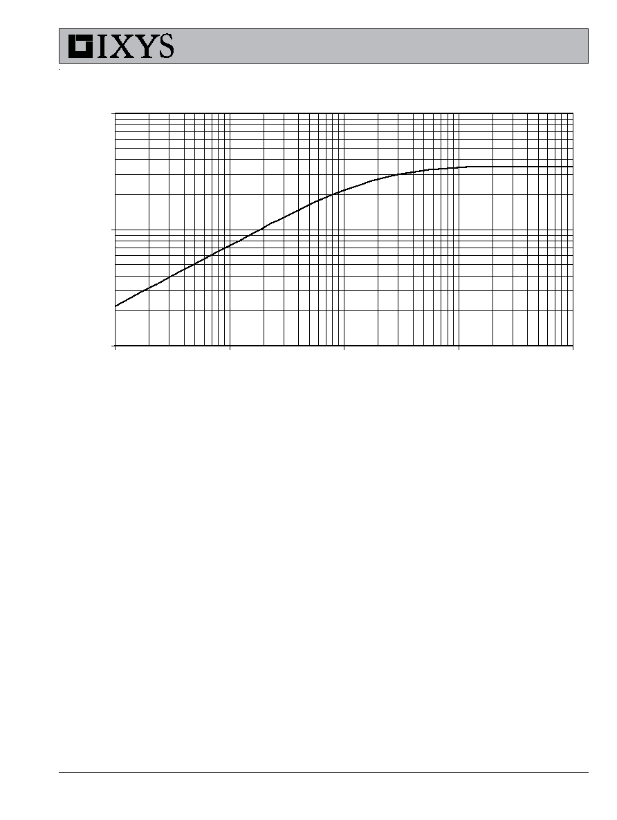
Fig. 9. Source Current vs.
Source-To-Drain Voltage
0
10
20
30
40
50
60
70
0.4
0.5
0.6
0.7
0.8
0.9
1
1.1
V
S D
- Volts
I
S
- A
m
p
e
re
s
T
J
= 125
C
T
J
= 25
C
Fig. 12. Forw ard-Bias
Safe Operating Area
1
10
100
10
100
1000
V
D S
- Volts
I
D
-
A
m
per
es
100µs
1ms
DC
T
J
= 150C
T
C
= 25C
R
DS(on)
Limit
10ms
25µs
© 2005 IXYS All rights reserved
Fig. 13. Maximum Transient Thermal Resistance
0.01
0.10
1.00
0.1
1
10
100
1000
Pulse Width - milliseconds
R
( t h ) J C
-
C / W
IXTQ 22N50P
IXTV 22N50PS IXTV 22N50P