 | –≠–ª–µ–∫—Ç—Ä–æ–Ω–Ω—ã–π –∫–æ–º–ø–æ–Ω–µ–Ω—Ç: IXTY3N60P | –°–∫–∞—á–∞—Ç—å:  PDF PDF  ZIP ZIP |
© 2005 IXYS All rights reserved
Symbol
Test Conditions
Maximum Ratings
V
DSS
T
J
= 25
∞C to 150∞C
600
V
V
DGR
T
J
= 25
∞C to 150∞C; R
GS
= 1 M
600
V
V
GS
Continuous
± 30
V
V
GSM
Transient
± 40
V
I
D25
T
C
= 25
∞C
2.8
A
I
DM
T
C
= 25
∞C, pulse width limited by T
JM
6
A
I
AR
T
C
= 25
∞C
3
A
E
AR
T
C
= 25
∞C
10
mJ
E
AS
T
C
= 25
∞C
180
mJ
dv/dt
I
S
I
DM
, di/dt
100 A/s, V
DD
V
DSS
5
V/ns
T
J
150∞C, R
G
= 20
P
D
T
C
= 25
∞C
70
W
T
J
-55 ... +150
∞C
T
JM
150
∞C
T
stg
-55 ... +150
∞C
T
L
1.6 mm (0.062 in.) from case for 10 s
300
∞C
Plastic body for 10 seconds
260
∞C
Weight
TO-220
4
g
TO-263
3
g
TO-252
0.35
g
Symbol
Test Conditions
Characteristic Values
(T
J
= 25
∞C unless otherwise specified)
Min. Typ.
Max.
V
DSS
V
GS
= 0 V, I
D
= 250
A
600
V
V
GS(th)
V
DS
= V
GS
, I
D
= 50
A
3.0
5.5
V
I
GSS
V
GS
=
± 30 V
DC
, V
DS
= 0
± 100
nA
I
DSS
V
DS
= V
DSS
5
A
V
GS
= 0 V
T
J
= 125
∞C
50
A
R
DS(on)
V
GS
= 10 V, I
D
= 0.5 I
D25
, Note 1
2.8
PolarHV
TM
Power
MOSFET
Advance Technical Information
N-Channel Enhancement Mode
Avalanche Rated
Fast Intrinsic Diode
Features
International standard packages
Unclamped Inductive Switching (UIS)
rated
Low package inductance
- easy to drive and to protect
Advantages
Easy to mount
Space savings
High power density
IXTA 3N60P
IXTP 3N60P
IXTY 3N60P
V
DSS
= 600
V
I
D25
= 2.8
A
R
DS(on)
2.8
DS99449B(10/05)
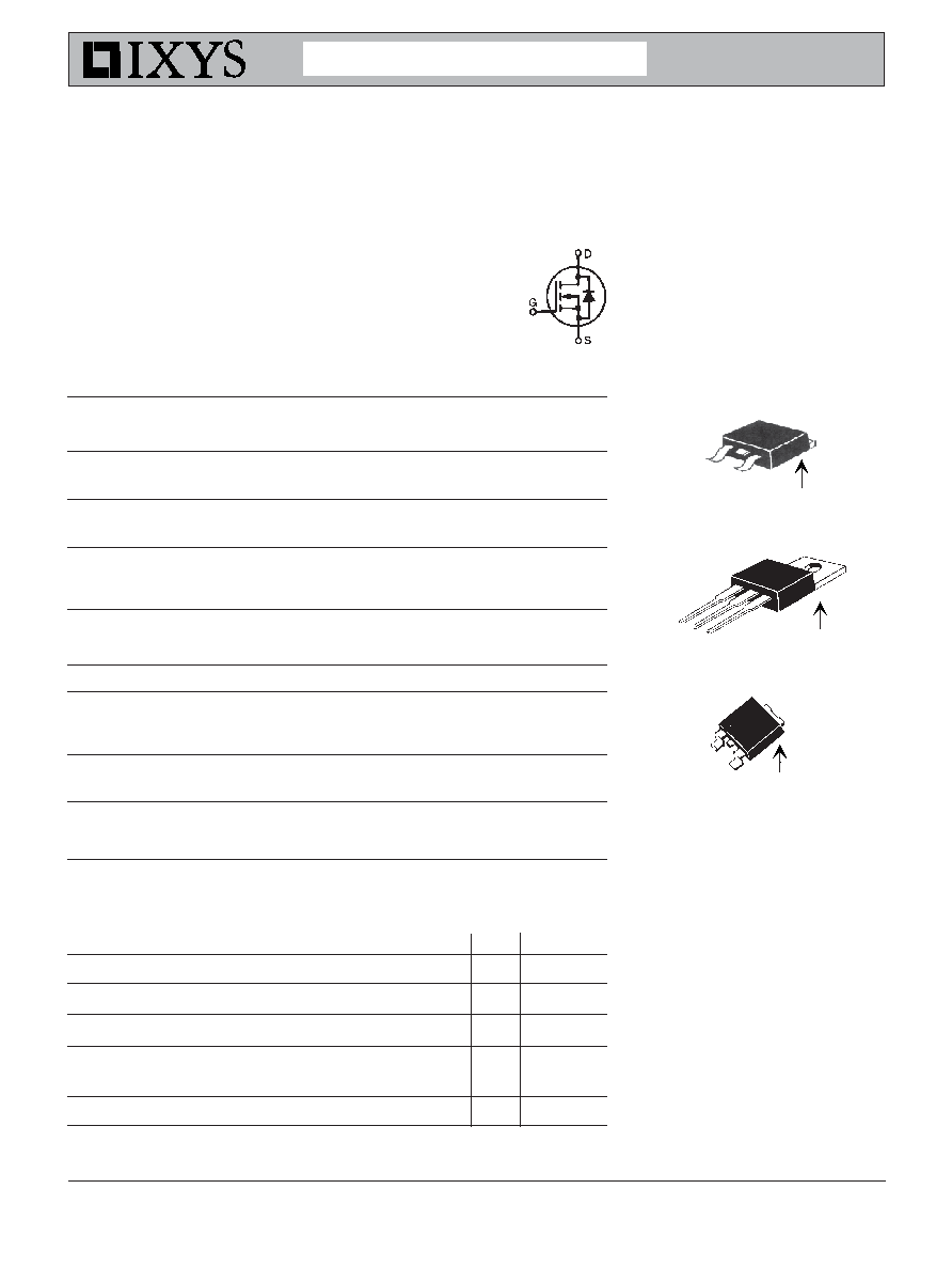
G = Gate
D = Drain
S = Source
TAB = Drain
TO-220 (IXTP)
S
TO-252 (IXTY)
(TAB)
TO-263 (IXTA)
G
S
D
G
(TAB)
G
S
(TAB)
IXYS reserves the right to change limits, test conditions, and dimensions.
IXTA 3N60P IXTP 3N60P
IXTY 3N60P
IXYS MOSFETs and IGBTs are covered by 4,835,592
4,931,844
5,049,961
5,237,481
6,162,665
6,404,065 B1
6,683,344
6,727,585
one or more of the following U.S. patents:
4,850,072
5,017,508
5,063,307
5,381,025
6,259,123 B1
6,534,343
6,710,405B2
6,759,692
4,881,106
5,034,796
5,187,117
5,486,715
6,306,728 B1
6,583,505
6,710,463
6771478 B2
Symbol
Test Conditions Characteristic Values
(T
J
= 25
∞C unless otherwise specified)
Min.
Typ.
Max.
g
fs
V
DS
= 20 V; I
D
= 0.5 I
D25
, Note 1
3.4
S
C
iss
411
pF
C
oss
V
GS
= 0 V, V
DS
= 25 V, f = 1 MHz
44
pF
C
rss
6.4
pF
t
d(on)
15
ns
t
r
V
GS
= 10 V, V
DS
= 0.5 V
DSS
, I
D
= I
D25
15
ns
t
d(off)
R
G
= 20
(External)
38
ns
t
f
12
ns
Q
g(on)
9.8
nC
Q
gs
V
GS
= 10 V, V
DS
= 0.5 V
DSS
, I
D
= 0.5 I
D25
3.4
nC
Q
gd
3.5
nC
R
thJC
1.8 K/W
R
thCH
(TO-220)
0.25
KW
Source-Drain Diode Characteristic Values
T
J
= 25
∞C unless otherwise specified)
Symbol
Test Conditions
Min.
Typ.
Max.
I
S
V
GS
= 0 V
3
A
I
SM
Repetitive
5
A
V
SD
I
F
= I
S
, V
GS
= 0 V, Note 1
1.5
V
t
rr
I
F
= 3 A, -di/dt = 100 A/
s
400
ns
V
R
= 100 V, V
GS
= 0 V
Note 1:
Pulse test, t
300 s, duty cycle d 2 %
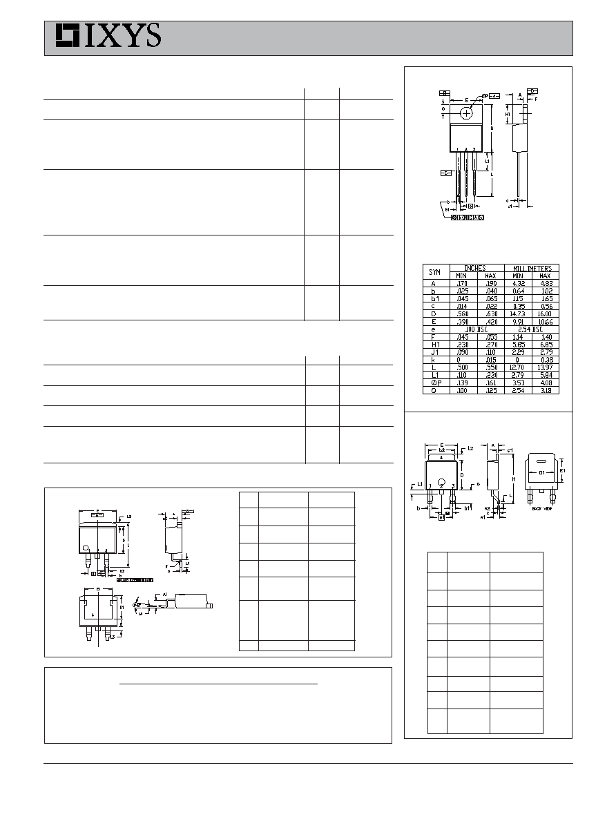
Dim. Millimeter
Inches
Min.
Max.
Min.
Max.
A
2.19
2.38
0.086
0.094
A1
0.89
1.14
0.035
0.045
A2
0
0.13
0
0.005
b
0.64
0.89
0.025
0.035
b1
0.76
1.14
0.030
0.045
b2
5.21
5.46
0.205
0.215
c
0.46
0.58
0.018
0.023
c1
0.46
0.58
0.018
0.023
D
5.97
6.22
0.235
0.245
D1
4.32
5.21
0.170
0.205
E
6.35
6.73
0.250
0.265
E1
4.32
5.21
0.170
0.205
e
2.28 BSC
0.090 BSC
e1
4.57 BSC
0.180 BSC
H
9.40 10.42
0.370
0.410
L
0.51
1.02
0.020
0.040
L1
0.64
1.02
0.025
0.040
L2
0.89
1.27
0.035
0.050
L3
2.54
2.92
0.100
0.115
TO-252AA Outline
Pins: 1 - Gate
2 - Drain
3 - Source
4 - Drain
TO-220AB (IXTP) Outline
Pins: 1 - Gate
3 - Source
4 - Drain
TO-263 AA (IXTA)
Outline
Dim.
Millimeter
Inches
Min.
Max.
Min.
Max.
A
4.06
4.83
.160
.190
A1
2.03
2.79
.080
.110
b
0.51
0.99
.020
.039
b2
1.14
1.40
.045
.055
c
0.46
0.74
.018
.029
c2
1.14
1.40
.045
.055
D
8.64
9.65
.340
.380
D1
7.11
8.13
.280
.320
E
9.65
10.29
.380
.405
E1
6.86
8.13
.270
.320
e
2.54
BSC
.100
BSC
L
14.61
15.88
.575
.625
L1
2.29
2.79
.090
.110
L2
1.02
1.40
.040
.055
L3
1.27
1.78
.050
.070
L4
0
0.38
0
.015
R
0.46
0.74
.018
.029
ADVANCE TECHNICAL INFORMATION
The product presented herein is under development. The Technical Specifications offered are
derived from a subjective evaluation of the design, based upon prior knowledge and experience,
and constitute a "considered reflection" of the anticipated objective result. IXYS reserves the right
to change limits, test conditions, and dimensions without notice.
Pins: 1 - Gate
2, 4 - Drain
3 - Source

© 2005 IXYS All rights reserved
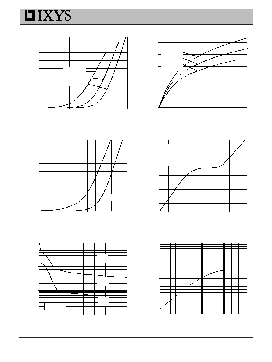
Fig. 2. Extended Output Characteristics
@ 25
∫
C
0
0.5
1
1.5
2
2.5
3
3.5
4
4.5
5
5.5
6
0
3
6
9
12
15
18
21
24
27
30
V
D S
- Volts
I
D
- A
m
p
e
re
s
V
GS
= 10V
8V
7V
6V
Fig. 3. Output Characteristics
@ 125
∫
C
0
0.3
0.6
0.9
1.2
1.5
1.8
2.1
2.4
2.7
3
0
2
4
6
8
10
12
14
16
18
20
V
D S
- Volts
I
D
-
A
m
per
e
s
V
GS
= 10V
8V
7V
5V
6V
Fig. 1. Output Characteristics
@ 25
∫
C
0
0.3
0.6
0.9
1.2
1.5
1.8
2.1
2.4
2.7
3
0
1
2
3
4
5
6
7
8
9
10
V
D S
- Volts
I
D
- A
m
p
e
re
s
V
GS
= 10V
8V
7V
6V
Fig. 4. R
DS(on
)
Norm alized to 0.5 I
D25
Value vs. Junction Tem perature
0.4
0.7
1
1.3
1.6
1.9
2.2
2.5
2.8
3.1
-50
-25
0
25
50
75
100
125
150
T
J
- Degrees Centigrade
R
D S
(
o
n
)
-
N
o
rm
a
l
i
z
e
d
I
D
= 3A
I
D
= 1.5A
V
GS
= 10V
Fig. 6. Drain Current vs. Case
Tem perature
0
0.3
0.6
0.9
1.2
1.5
1.8
2.1
2.4
2.7
3
3.3
-50
-25
0
25
50
75
100
125
150
T
C
- Degrees Centigrade
I
D
-
A
m
per
es
Fig. 5. R
DS(on)
Norm alized to
0.5 I
D25
Value vs. I
D
0.8
1
1.2
1.4
1.6
1.8
2
2.2
2.4
2.6
2.8
3
0
1
2
3
4
5
6
I
D
- Amperes
R
D S
(
o
n
)
-
N
o
r
m
aliz
e
d
T
J
= 125
∫
C
T
J
= 25
∫
C
V
GS
= 10V
IXTA 3N60P IXTP 3N60P
IXTY 3N60P
IXYS reserves the right to change limits, test conditions, and dimensions.
IXTA 3N60P IXTP 3N60P
IXTY 3N60P
IXYS MOSFETs and IGBTs are covered by 4,835,592
4,931,844
5,049,961
5,237,481
6,162,665
6,404,065 B1
6,683,344
6,727,585
one or more of the following U.S. patents:
4,850,072
5,017,508
5,063,307
5,381,025
6,259,123 B1
6,534,343
6,710,405B2
6,759,692
4,881,106
5,034,796
5,187,117
5,486,715
6,306,728 B1
6,583,505
6,710,463
6771478 B2
Fig. 11. Capacitance
1
10
100
1000
0
5
10
15
20
25
30
35
40
V
D S
- Volts
C
a
pa
c
i
t
a
n
c
e -
pi
c
o
F
a
r
a
d
s
Ciss
Coss
Crss
f = 1MHz
Fig. 10. Gate Charge
0
1
2
3
4
5
6
7
8
9
10
0
1
2
3
4
5
6
7
8
9
10
Q
G
- nanoCoulombs
V
G S
- V
o
l
t
s
V
DS
= 300V
I
D
= 1.5A
I
G
= 10mA
Fig. 7. Input Adm ittance
0
0.5
1
1.5
2
2.5
3
3.5
4
4.5
4
4.5
5
5.5
6
6.5
7
V
G S
- Volts
I
D
- A
m
p
e
r
e
s
T
J
=125
∫
C
25
∫
C
-40
∫
C
Fig. 8. Transconductance
0
0.5
1
1.5
2
2.5
3
3.5
4
4.5
5
5.5
6
0
0.5
1
1.5
2
2.5
3
3.5
4
I
D
- Amperes
g
f s
- S
i
e
m
e
n
s
T
J
= -40
∫
C
25
∫
C
125
∫
C
Fig. 9. Source Current vs.
Source-To-Drain Voltage
0
1
2
3
4
5
6
7
8
9
0.4
0.5
0.6
0.7
0.8
0.9
V
S D
- Volts
I
S
- A
m
p
e
re
s
T
J
= 125
∫
C
T
J
= 25
∫
C
Fig. 13. Maxim um Transient Therm al
Resistance
0.1
1.0
10.0
0.1
1
10
100
1000
Pulse Width - milliseconds
R
( t
h
)
J
C
-
∫
C /
W