© 2004 IXYS All rights reserved
1 - 2
IXYS reserves the right to change limits, test conditions and dimensions.
VBO 50
420
V
RSM
V
RRM
Type
V
V
800
800
VBO 50-08NO7
1200
1200
VBO 50-12NO7
1400
1400
VBO 50-14NO7
1600
1600
VBO 50-16NO7
1800
1800
VBO 50-18NO7*
Symbol
Conditions
Maximum Ratings
I
dAVM
T
C
= 64
∞C, module
50
A
I
FSM
T
VJ
= 45
∞C;
t = 10 ms (50 Hz), sine
750
A
V
R
= 0
t = 8.3 ms (60 Hz), sine
820
A
T
VJ
= T
VJM
t = 10 ms (50 Hz), sine
670
A
V
R
= 0
t = 8.3 ms (60 Hz), sine
740
A
I
2
t
T
VJ
= 45
∞C
t = 10 ms (50 Hz), sine
2800
A
2
s
V
R
= 0
t = 8.3 ms (60 Hz), sine
2820
A
2
s
T
VJ
= T
VJM
t = 10 ms (50 Hz), sine
2250
A
2
s
V
R
= 0
t = 8.3 ms (60 Hz), sine
2300
A
2
s
T
VJ
-40...+150
∞C
T
VJM
150
∞C
T
stg
-40...+150
∞C
V
ISOL
50/60 Hz, RMS
t = 1 min
2500
V~
I
ISOL
1 mA
t = 1 s
3000
V~
M
d
Mounting torque (M5)
5
±15%
Nm
44
±15% lb.in.
Terminal connection torque (M5)
3
±15%
Nm
26
±15% lb.in.
Weight
typ.
260
g
Features
∑ Package with screw terminals
∑ Isolation voltage 3000 V~
∑ Planar passivated chips
∑ Blocking voltage up to 1800 V
∑ Low forward voltage drop
∑ UL registered E 72873
Applications
∑ Supplies for DC power equipment
∑ Input rectifiers for PWM inverter
∑ Battery DC power supplies
∑ Field supply for DC motors
Advantages
∑ Easy to mount with two screws
∑ Space and weight savings
∑ Improved temperature and power cycling
Symbol
Conditions
Characteristic Values
I
R
V
R
= V
RRM
;
T
VJ
= 25
∞C
0.3
mA
V
R
= V
RRM
;
T
VJ
= T
VJM
10.0
mA
V
F
I
F
= 150 A;
T
VJ
= 25
∞C
1.6
V
V
T0
For power-loss calculations only
0.85
V
r
T
T
VJ
= T
VJM
8
m
R
thJC
per diode; DC current
2.6
K/W
per module
0.65
K/W
R
thJK
per diode; DC current
2.84
K/W
per module
0.71
K/W
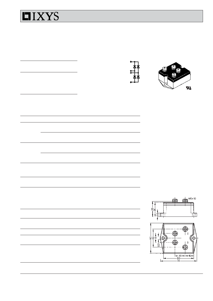
Dimensions in mm (1 mm = 0.0394")
Data according to IEC 60747 refer to a single diode unless otherwise stated.
I
dAVM
= 50 A
V
RRM
= 800-1800 V
Single Phase
Rectifier Bridge
~
+
~
-
* delivery time on request
+
≠
~
~

© 2004 IXYS All rights reserved
2 - 2
IXYS reserves the right to change limits, test conditions and dimensions.
VBO 50
420
Fig. 1 Forward current versus
voltage drop per diode
Fig. 2 Surge overload current per diode
I
FSM
: Crest value. t: duration
Fig.5 Maximum forward current
at case temperature
Fig. 4 Power dissipation versus direct output current and ambient temperature
Fig. 3
i
2
dt versus time
(1-10ms) per diode or thyristor
Fig. 6 Transient thermal impedance per diode or thyristor, calculated
0.5
1
1.5
2
2.5
0
50
100
150
200
V [V]
F
I
F
[A]
1:T = 150∞
VJ
C
2:T = 25∞C
VJ
1
2
0.4
0.6
0.8
1
1.2
1.4
1.6
10
0
10
1
10
2
10
3
t[ms]
I (A)
FSM
TVJ=45∞C TVJ=150∞C
750 670
I
------
I
FSM
F(OV)
0 V
RRM
1/2 V
RRM
1 V
RRM
2
4
6
10
TVJ=45∞C
TVJ=150∞C
t [ms]
1
10
10
10
2
3
4
As
2
50
100
150
200
0
10
30
50
70
DC
sin.180∞
rec.120∞
c.60∞
re
.30∞
T (∞C)
C
I
dAV
[A]
0.01
0.1
1
10
1
2
3
4
K/W
Zth
t[s]
Z thJK
Z thJC
30
10
0
20
40
60
80
100
85
90
95
100
105
110
115
120
125
130
135
140
145
150
TC
∞C
DC
sin.180∞
rec.120∞
rec.60∞
rec.30∞
5.35
2.35
1.35
0.85
0.6 0.35
= RTHCA [K/W]
IFAVM
[A]
Tamb
[K]
0
50
100
150
[W]
PVTOT
PSB 55