 | –≠–ª–µ–∫—Ç—Ä–æ–Ω–Ω—ã–π –∫–æ–º–ø–æ–Ω–µ–Ω—Ç: L486 | –°–∫–∞—á–∞—Ç—å:  PDF PDF  ZIP ZIP |
© 2004 IXYS All rights reserved
1 - 4
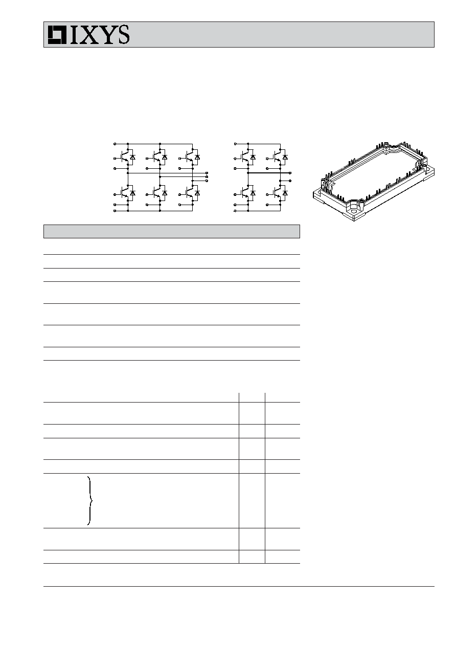
MWI 100-12 E8
MKI 100-12 E8
448
IXYS reserves the right to change limits, test conditions and dimensions.
Features
∑ NPT
3
IGBTs
- low saturation voltage
- positive temperature coefficient for
easy paralleling
- fast switching
- short tail current for optimized
performance also in resonant circuits
∑ HiPerFRED
TM
diode:
- fast reverse recovery
- low operating forward voltage
- low leakage current
∑ Industry Standard Package
- solderable pins for PCB mounting
- isolated copper base plate
Typical Applications
∑ MWI
- AC drives
- power supplies with power factor
correction
∑ MKI
- motor control
. DC motor amature winding
. DC motor excitation winding
. synchronous motor excitation winding
- supply of transformer primary winding
. power supplies
. welding
. X-ray
. battery charger
I
C25
= 165 A
V
CES
= 1200 V
V
CE(sat) typ.
= 2.0 V
IGBT Modules
Sixpack, H Bridge
Short Circuit SOA Capability
Square RBSOA
13, 21
14, 20
1
2
3
4
7
8
9
10
11
12
5
6
17
19
15
MWI
IGBTs
Symbol
Conditions
Maximum Ratings
V
CES
T
VJ
= 25∞C to 150∞C
1200
V
V
GES
± 20
V
I
C25
T
C
= 25∞C
165
A
I
C80
T
C
= 80∞C
115
A
I
CM
V
GE
=
±15 V; R
G
= 12
; T
VJ
= 125∞C
200
A
V
CEK
RBSOA; clamped inductive load; L = 100 µH
V
CES
t
SC
V
CE
= 900 V; V
GE
=
±15 V; R
G
= 12
; T
VJ
= 125∞C
10
µs
SCSOA; non-repetitive
P
tot
T
C
= 25∞C
640
W
Symbol
Conditions
Characteristic Values
(T
VJ
= 25
∞C, unless otherwise specified)
min.
typ.
max.
V
CE(sat)
I
C
= 100 A; V
GE
= 15 V; T
VJ
= 25∞C
2.0
2.5
V
T
VJ
= 125∞C
2.3
V
V
GE(th)
I
C
= 4 mA; V
GE
= V
CE
4.5
6.5
V
I
CES
V
CE
= V
CES
;
V
GE
= 0 V;
T
VJ
= 25∞C
1.4
mA
T
VJ
= 125∞C
1.4
mA
I
GES
V
CE
= 0 V; V
GE
=
± 20 V
400
nA
t
d(on)
330
ns
t
r
15
ns
t
d(off)
750
ns
t
f
45
ns
E
on
12
mJ
E
off
10
mJ
C
ies
V
CE
= 25 V; V
GE
= 0 V; f = 1 MHz
7.4
nF
Q
Gon
V
CE
= 600 V; V
GE
= 15 V; I
C
= 150 A
0.76
µC
R
thJC
(per IGBT)
0.19 K/W
Inductive load, T
VJ
= 125∞C
V
CE
= 600 V; I
C
= 100 A
V
GE
= ±15 V; R
G
= 12
MKI
19
15
9
10
11
12
13, 21
14, 20
1
2
3
4
© 2004 IXYS All rights reserved
2 - 4
MWI 100-12 E8
MKI 100-12 E8
448
IXYS reserves the right to change limits, test conditions and dimensions.
Equivalent Circuits for Simulation
Conduction
IGBT (typ. at V
GE
= 15 V; T
J
= 125∞C)
V
0
= 0.95 V; R
0
= 14 m
Free Wheeling Diode (typ. at T
J
= 125∞C)
V
0
= 1.3 V; R
0
= 7 m
Thermal Response
IGBT (typ.)
C
th1
= 0.389 J/K; R
th1
= 0.139 K/W
C
th2
= 2.154 J/K; R
th2
= 0.051 K/W
Free Wheeling Diode (typ.)
C
th1
= 0.301 J/K; R
th1
= 0.24 K/W
C
th2
= 2.005 J/K; R
th2
= 0.062 K/W
Module
Symbol
Conditions
Maximum Ratings
T
VJ
operating
-40...+125
∞C
T
JM
+150
∞C
T
stg
-40...+125
∞C
V
ISOL
I
ISOL
1 mA; 50/60 Hz
2500
V~
M
d
Mounting torque (M5)
2.7 - 3.3
Nm
Symbol
Conditions
Characteristic Values
min.
typ.
max.
R
pin-chip
1.8
m
d
S
Creepage distance on surface
10
mm
d
A
Strike distance in air
10
mm
R
thCH
with heatsink compound
0.01
K/W
Weight
300
g
Diodes
Symbol
Conditions
Maximum Ratings
I
F25
T
C
= 25∞C
200
A
I
F80
T
C
= 80∞C
130
A
Symbol
Conditions
Characteristic Values
min.
typ.
max.
V
F
I
F
= 100 A; V
GE
= 0 V; T
VJ
= 25∞C
2.3
2.6
V
T
VJ
= 125∞C
1.7
V
I
RM
I
F
= 120 A; di
F
/dt = -750 A/µs; T
VJ
= 125∞C
58
A
t
rr
V
R
= 600 V; V
GE
= 0 V
190
ns
R
thJC
(per diode)
0.3 K/W
pins 5, 6, 7, 8 and 17 for MWI only
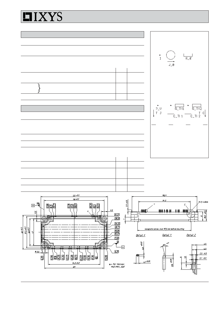
Dimensions in mm (1 mm = 0.0394")

© 2004 IXYS All rights reserved
3 - 4
MWI 100-12 E8
MKI 100-12 E8
448
IXYS reserves the right to change limits, test conditions and dimensions.
0
200
400
600
800
1000
0
30
60
90
0
50
100
150
200
250
300
0
1
2
3
4
5
0
50
100
150
200
250
300
0
200
400
600
800
1000
0
5
10
15
20
0
1
2
3
4
5
0
50
100
150
200
250
300
V
CE
V
I
C
V
CE
A
I
C
V
nC
Q
G
-di/dt
V
V
GE
I
RM
t
rr
A/
µs
MWI100-12E8
I
RM
t
rr
A
9 V
11 V
A
5
6
7
8
9
10
0
50
100
150
200
250
300
V
V
GE
A
I
C
0
1
2
3
0
50
100
150
200
250
300
V
V
F
I
F
A
ns
15 V
T
VJ
= 25∞C
9 V
11 V
13 V
V
GE
= 17 V
T
VJ
= 125∞C
T
VJ
= 125∞C
T
VJ
= 25∞C
V
CE
= 20 V
T
VJ
= 125∞C
T
VJ
= 25∞C
13 V
V
GE
= 17 V
15 V
T
VJ
= 125∞C
V
R
= 600 V
I
F
= 120 A
V
CE
= 600 V
I
C
= 150 A
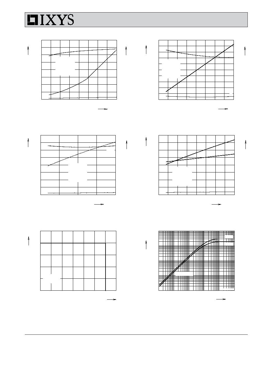
Fig. 1 Typ. output characteristics
Fig. 2
Typ. output characteristics
Fig. 3 Typ. transfer characteristics
Fig. 4
Typ. forward characteristics
of free wheeling diode
Fig. 5 Typ. turn on gate charge
Fig. 6
Typ. turn off characteristics
of free wheeling diode
© 2004 IXYS All rights reserved
4 - 4
MWI 100-12 E8
MKI 100-12 E8
448
IXYS reserves the right to change limits, test conditions and dimensions.
0
50
100
150
200
0
10
20
30
40
0
100
200
300
400
0
50
100
150
200
0
4
8
12
16
20
0
200
400
600
800
1000
0.0001
0.001
0.01
0.1
1
10
0.0001
0.001
0.01
0.1
1
0
5
10
15
20
0
4
8
12
16
0
250
500
750
1000
0
5
10
15
20
0
4
8
12
16
0
100
200
300
400
0
200
400
600
800 1000 1200 1400
0
50
100
150
200
250
Eoff
td(off)
Eoff
td(off)
I
C
A
I
C
A
E
off
E
on
t
t
R
G
R
G
V
CE
t
s
mJ
E
on
mJ
E
off
t
ns
t
I
CM
K/W
Z
thJC
V
A
mJ
ns
mJ
ns
tr
Eon
tr
single pulse
diode
IGBT
ns
Eon
MWI100-12E8
td(on)
tf
V
CE
= 600 V
V
GE
= ±15 V
I
C
= 100 A
T
VJ
= 125∞C
V
CE
= 600 V
V
GE
= ±15 V
I
C
= 100 A
T
VJ
= 125∞C
V
CE
= 600 V
V
GE
= ±15 V
R
G
= 12
T
VJ
= 125∞C
V
CE
= 600 V
V
GE
= ±15 V
R
G
= 12
T
VJ
= 125∞C
R
G
= 12
T
VJ
= 125∞C
td(on)
tf
Fig. 7
Typ. turn on energy and switching
Fig. 8
Typ. turn off energy and switching
times versus collector current
times versus collector current
Fig. 9
Typ. turn on energy and switching
Fig.10 Typ. turn off energy and switching
times versus gate resistor
times versus gate resistor
Fig. 11 Reverse biased safe operating area
Fig. 12 Typ. transient thermal impedance
RBSOA