© 2002 IXYS All rights reserved
1 - 1
IXYS reserves the right to change limits, test conditions and dimensions.
VUO 122
241
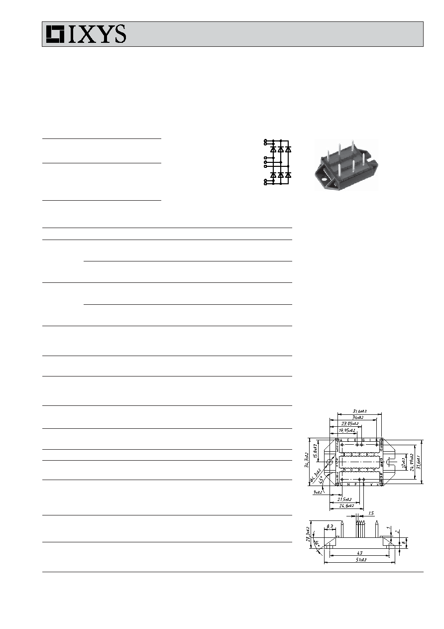
B3
Three Phase Rectifier Bridge
in ECO-PAC 2
I
dAV
= 117 A
V
RRM
= 800-1600 V
V
RSM
V
RRM
Types
V
V
900
800
VUO 122-08NO7
1300
1200
VUO 122-12NO7
1500
1400
VUO 122-14NO7
1700
1600
VUO 122-16NO7
Symbol
Test Conditions
Maximum Ratings
I
dAV
T
C
= 100∞C, module
117
A
I
FSM
T
VJ
= 45∞C;
t = 10 ms (50 Hz), sine
900
A
V
R
= 0
t = 8.3 ms (60 Hz), sine
990
A
T
VJ
= T
VJM
t = 10 ms (50 Hz), sine
770
A
V
R
= 0
t = 8.3 ms (60 Hz), sine
850
A
I
2
t
T
VJ
= 45∞C
t = 10 ms (50 Hz), sine
4050
A
2
s
V
R
= 0
t = 8.3 ms (60 Hz), sine
4050
A
2
s
T
VJ
= T
VJM
t = 10 ms (50 Hz), sine
2950
A
2
s
V
R
= 0
t = 8.3 ms (60 Hz), sine
2950
A
2
s
T
VJ
-40...+150
∞C
T
VJM
150
∞C
T
stg
-40...+125
∞C
V
ISOL
50/60 Hz, RMS
t = 1 min
2500
V~
I
ISOL
1 mA
t = 1 s
3000
V~
M
d
Mounting torque (M4)
1.5 - 2
Nm
14 - 18
lb.in.
Weight
typ.
18
g
Symbol
Test Conditions
Characteristic Values
I
R
V
R
= V
RRM
;
T
VJ
= 25∞C
0.5
mA
V
R
= V
RRM
;
T
VJ
= T
VJM
5
mA
V
F
I
F
= 200 A;
T
VJ
= 25∞C
1.75
V
V
T0
For power-loss calculations only
0.8
V
r
T
4
m
R
thJC
per diode; DC current
0.85
K/W
per module
0.142
K/W
R
thJH
per diode, DC current (typ.)
1.15
K/W
per module (typ.)
0.192
K/W
d
S
Creeping distance on surface
11.2
mm
d
A
Creepage distance in air
9.7
mm
a
Max. allowable acceleration
50
m/s
2
Features
∑ Package with DCB ceramic
base plate
∑ Isolation voltage 3000 V~
∑ Planar passivated chips
∑ Low forward voltage drop
∑ Leads suitable for PC board soldering
Applications
∑ Supplies for DC power equipment
∑ Input rectifiers for PWM inverter
∑ Battery DC power supplies
∑ Field supply for DC motors
Advantages
∑ Easy to mount with two screws
∑ Space and weight savings
∑ Improved temperature and power
cycling capability
∑ Small and light weight
Dimensions in mm (1 mm = 0.0394")
Data according to IEC 60747 refer to a single diode unless otherwise stated
for resistive load at bridge output.
Preliminary data
PS16
EG 1
~
A 1
~
L 9
~
K10
Pin arangement see outlines