© 2000 IXYS All rights reserved
1 - 4
V
RSM
V
RRM
Type
V
DSM
V
DRM
V
V
1300
1200
MCC 170-12io1
1500
1400
MCC 170-14io1
1700
1600
MCC 170-16io1
1900
1800
MCC 170-18io1
Symbol
Test Conditions
Maximum Ratings
I
TRMS
T
VJ
= T
VJM
350
A
I
TAVM
T
C
= 85
∞
C; 180
∞
sine
203
A
I
TSM
, I
FSM
T
VJ
= 45
∞
C;
t = 10 ms (50 Hz)
5400
A
V
R
= 0
t = 8.3 ms (60 Hz)
5800
A
T
VJ
= T
VJM
t = 10 ms (50 Hz)
5000
A
V
R
= 0
t = 8.3 ms (60 Hz)
5500
A
Ú
i
2
dt
T
VJ
= 45
∞
C
t = 10 ms (50 Hz)
146 000
A
2
s
V
R
= 0
t = 8.3 ms (60 Hz)
140 000
A
2
s
T
VJ
= T
VJM
t = 10 ms (50 Hz)
125 000
A
2
s
V
R
= 0
t = 8.3 ms (60 Hz)
126 000
A
2
s
(di/dt)
cr
T
VJ
= T
VJM
repetitive, I
T
= 660 A
100
A/
m
s
f =50 Hz, t
P
=200
m
s
V
D
= 2/3 V
DRM
I
G
= 1 A,
non repetitive, I
T
= I
TAVM
500
A/
m
s
di
G
/dt = 1 A/
m
s
(dv/dt)
cr
T
VJ
= T
VJM
; V
DR
= 2/3 V
DRM
1000
V/
m
s
R
GK
=
•
; method 1 (linear voltage rise)
P
GM
T
VJ
= T
VJM
t
P
=
30
m
s
120
W
I
T
= I
TAVM
t
P
= 500
m
s
60
W
P
GAV
20
W
V
RGM
10
V
T
VJ
-40...+130
∞
C
T
VJM
130
∞
C
T
stg
-40...+125
∞
C
V
ISOL
50/60 Hz, RMS
t = 1 min
3000
V~
I
ISOL
£
1 mA
t = 1 s
3600
V~
M
d
Mounting torque (M6)
4.5-7/40-62 Nm/lb.in.
Terminal connection torque (M8)
11-13/97-115 Nm/lb.in.
Weight
Typical including screws
750
g
Features
q
International standard package
q
Direct copper bonded Al
2
O
3
-ceramic
with copper base plate
q
Planar passivated chips
q
Isolation voltage 3600 V~
q
UL registered E 72873
q
Keyed gate/cathode twin pins
Applications
q
Motor control, softstarter
q
Power converter
q
Heat and temperature control for
industrial furnaces and chemical
processes
q
Lighting control
q
Solid state switches
Advantages
q
Simple mounting
q
Improved temperature and power
cycling
q
Reduced protection circuits
I
TRMS
= 2x 350 A
I
TAVM
= 2x 203 A
V
RRM
= 1200-1800 V
Data according to IEC 60747 and refer to a single thyristor/diode unless otherwise stated.
IXYS reserves the right to change limits, test conditions and dimensions
MCC 170
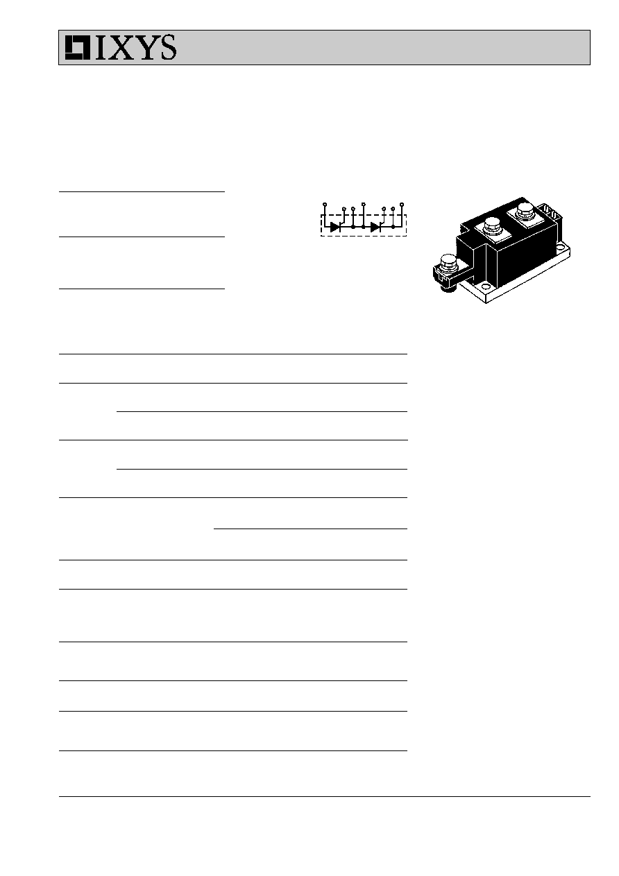
Thyristor Modules
Thyristor/Diode Modules
1
2
3
76
5
4
3
6 7 1
5 4 2
© 2000 IXYS All rights reserved
2 - 4
Symbol
Test Conditions
Characteristic Values
I
RRM
, I
DRM
T
VJ
= T
VJM
; V
R
= V
RRM
; V
D
= V
DRM
40
mA
V
T
, V
F
I
T
, I
F
= 600 A; T
VJ
= 25
∞
C
1.65
V
V
T0
For power-loss calculations only (T
VJ
= 130
∞
C)
0.8
V
r
T
1
m
W
V
GT
V
D
= 6 V;
T
VJ
= 25
∞
C
2
V
T
VJ
= -40
∞
C
3
V
I
GT
V
D
= 6 V;
T
VJ
= 25
∞
C
150
mA
T
VJ
= -40
∞
C
220
mA
V
GD
T
VJ
= T
VJM
;
V
D
= 2/3 V
DRM
0.25
V
I
GD
T
VJ
= T
VJM
;
V
D
= 2/3 V
DRM
10
mA
I
L
T
VJ
= 25
∞
C; t
P
= 30
m
s; V
D
= 6 V
200
mA
I
G
= 0.45 A; di
G
/dt = 0.45 A/
m
s
I
H
T
VJ
= 25
∞
C; V
D
= 6 V; R
GK
=
•
150
mA
t
gd
T
VJ
= 25
∞
C; V
D
= 1/2 V
DRM
2
m
s
I
G
= 1 A; di
G
/dt = 1 A/
m
s
t
q
T
VJ
= T
VJM
; I
T
= 300 A, t
P
= 200
m
s; -di/dt = 10 A/
m
s
typ.
200
m
s
V
R
= 100 V; dv/dt = 50 V/
m
s; V
D
= 2/3 V
DRM
Q
S
T
VJ
= 125
∞
C; I
T
, I
F
= 300 A; -di/dt = 50 A/
m
s
550
m
C
I
RM
235
A
R
thJC
per thyristor (diode); DC current
0.164
K/W
per module
other values
0.082
K/W
R
thJK
per thyristor (diode); DC current
see Fig. 8/9
0.204
K/W
per module
0.102
K/W
d
S
Creeping distance on surface
12.7
mm
d
A
Creepage distance in air
9.6
mm
a
Maximum allowable acceleration
50 m/s
2
Optional accessories for modules
Keyed Gate/Cathode twin plugs with wire length = 350 mm, gate = yellow, cathode = red
Type ZY 180 L (L = Left for pin pair 4/5)
UL 758, style 1385,
Type ZY 180 R (R = Right for pin pair 6/7)
CSA class 5851, guide 460-1-1
MCC 170
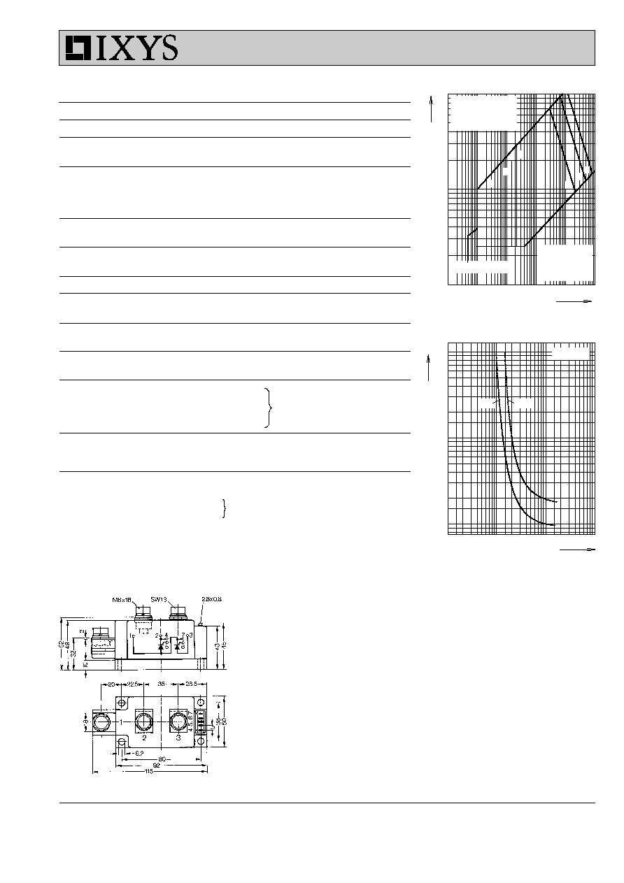
Fig. 1 Gate trigger characteristics
Fig. 2 Gate trigger delay time
0.01
0.1
1
10
1
10
100
10
-3
10
-2
10
-1
10
0
10
1
10
2
0.1
1
10
I
G
V
G
A
A
I
G
1: I
GT
, T
VJ
= 140
∞
C
2: I
GT
, T
VJ
= 25
∞
C
3: I
GT
, T
VJ
= -40
∞
C
µ
s
t
gd
V
4: P
GM
= 20 W
5: P
GM
= 60 W
6: P
GM
= 120 W
I
GD
, T
VJ
= 140
∞
C
4
2
1
5
6
Limit
typ.
T
VJ
= 25
∞
C
3
0.01
0.1
1
10
1
10
100
10
-3
10
-2
10
-1
10
0
10
1
10
2
0.1
1
10
I
G
V
G
A
A
I
G
1: I
GT
, T
VJ
= 130
∞
C
2: I
GT
, T
VJ
= 25
∞
C
3: I
GT
, T
VJ
= -40
∞
C
µ
s
t
gd
V
4: P
GM
= 20 W
5: P
GM
= 60 W
6: P
GM
= 120 W
I
GD
, T
VJ
= 130
∞
C
4
2
1
5
6
Limit
typ.
T
VJ
= 25
∞
C
3
Dimensions in mm (1 mm = 0.0394")
M8x20
© 2000 IXYS All rights reserved
3 - 4
I
TAVM
/I
FAVM
I
dAVM
P
tot
T
A
T
A
T
C
s
t
ms
t
0.001
0.01
0.1
1
0
1000
2000
3000
4000
5000
6000
1
10
10
4
10
5
10
6
A
2
s
0
25
50
75
100
125
150
0
100
200
300
400
I
TSM
A
A
∞C
I
TAVM
I
FAVM
0
25
50
75
100
125
150
0
100
200
300
0
100
200
300
400
W
P
tot
A
∞C
0
25
50
75
100
125
150
0
200
400
600
0
500
1000
1500
2000
∞C
I
2
dt
80 % V
RRM
T
VJ
= 45∞C
50 Hz
T
VJ
= 130∞C
T
VJ
= 130∞C
T
VJ
= 45∞C
R
thKA
K/W
0.1
0.2
0.3
0.4
0.6
0.8
1.0
A
W
R
thKA
K/W
0.3
0.1
0.15
0.2
0.06
0.08
0.04
180∞ sin
120∞
60∞
30∞
DC
180∞ sin
120∞
60∞
30∞
DC
B6
Circuit
3xMCC170
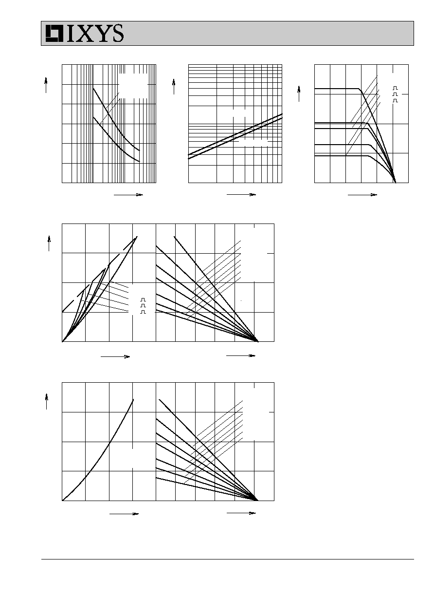
Fig. 3 Surge overload current
I
TSM
, I
FSM
: Crest value, t: duration
Fig. 4
Ú
i
2
dt versus time (1-10 ms)
Fig. 4a Maximum forward current
at case temperature
Fig. 5
Power dissipation versus on-
state current and ambient
temperature (per thyristor or
diode)
Fig. 6 Three phase rectifier bridge:
Power dissipation versus direct
output current and ambient
temperature
MCC 170
© 2000 IXYS All rights reserved
4 - 4
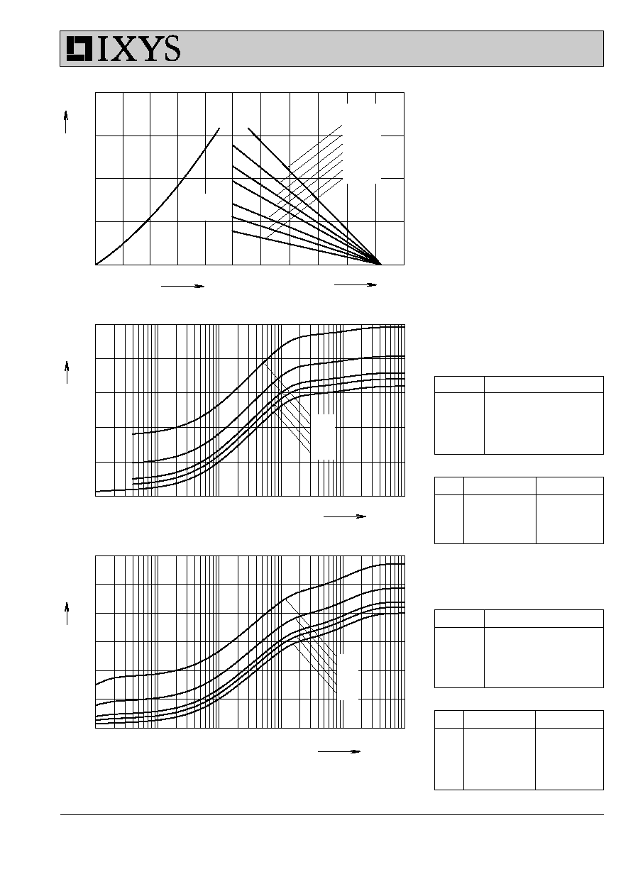
Fig. 7 Three phase AC-controller:
Power dissipation versus RMS
output current and ambient
temperature
Fig. 8 Transient thermal impedance
junction to case (per thyristor or
diode)
R
thJC
for various conduction angles d:
d
R
thJC
(K/W)
DC
0.160
180
∞
0.171
120
∞
0.180
60
∞
0.203
30
∞
0.247
Constants for Z
thJC
calculation:
i
R
thi
(K/W)
t
i
(s)
1
0.0077
0.00054
2
0.0413
0.098
3
0.096
0.54
4
0.0149
12
Fig. 9 Transient thermal impedance
junction to
heatsink
(per
thyristor
or diode)
R
thJK
for various conduction angles d:
d
R
thJK
(K/W)
DC
0.200
180
∞
0.211
120
∞
0.220
60
∞
0.243
30
∞
0.287
Constants for Z
thJK
calculation:
i
R
thi
(K/W)
t
i
(s)
1
0.0077
0.00054
2
0.0413
0.098
3
0.096
0.54
4
0.0149
12
5
0.04
12
MCC 170
0
100
200
300
400
0
500
1000
1500
2000
s
t
Z
thJK
s
t
10
-3
10
-2
10
-1
10
0
10
1
10
2
0.00
0.05
0.10
0.15
0.20
0.25
0.30
K/W
Z
thJC
K/W
I
RMS
P
tot
0
25
50
75
100
125
150
A
Circuit
W3
0.2
0.15
0.1
R
thKA
K/W
0.3
T
A
∞C
10
-3
10
-2
10
-1
10
0
10
1
10
2
0.00
0.05
0.10
0.15
0.20
0.25
3xMCC170
0.04
0.06
0.08
W
DC
180∞
120∞
60∞
30∞
DC
180∞
120∞
60∞
30∞