© 2000 IXYS All rights reserved
1 - 8
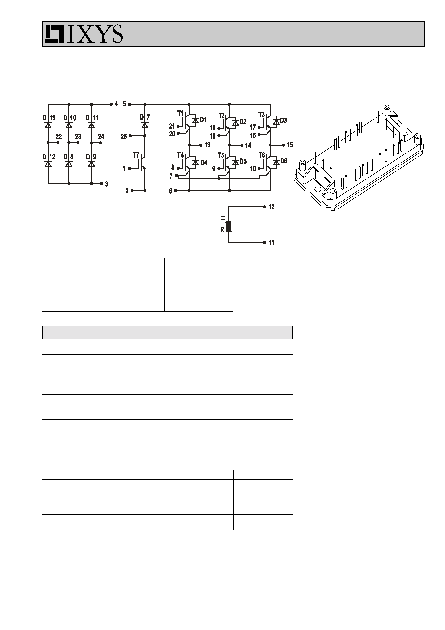
MUBW 15-12 A6
Input Rectifier Bridge D8 - D13
Symbol
Conditions
Maximum Ratings
V
RRM
1600
V
I
F
T
VJ
= 25∞C
55
A
I
FAVM
T
VJ
= 150∞C; T
K
= 70∞C
25
A
I
FSM
T
VJ
= 45∞C; t = 10 ms sine 50 Hz
370
A
i≤t
T
VJ
= 125∞C
680
A≤s
T
VJ
+150
∞C
Symbol
Conditions
Characteristic Values
(T
VJ
= 25
∞
C, unless otherwise specified)
min.
typ.
max.
I
R
V
RRM
= 1200 V; T
VJ
= 25∞C
20
µA
T
VJ
= 125∞C
2
mA
V
F
I
F
= 55 A
1.2
1.46
V
R
thJC
per die
1.05
∞C/W
Rectifier
Brake
Inverter
V
RRM
= 1600V
V
CES
= 1200 V
V
CES
= 1200 V
I
FAVM
= 25 A
I
C25
= 13 A
I
C25
= 18 A
I
FSM
= 370 A
V
CE(sat)
= 2.8 V
V
CE(sat)
= 2.8 V
IXYS reserves the right to change limits, test conditions and dimensions.
Converter - Brake - Inverter Module (CBI1)
Features
q
NPT IGBT technology
Square RBSOA, no latchup
q
Free wheeling diodes with Hiperfast
and soft recovery behaviour
q
Isolation voltage 2500 V~
q
Built in temperature sense
q
High level of integration:
one module for complete drive
system
q
Direct Copper Bonded Al
2
O
3
ceramic
base plate
Applications
q
AC motor control
q
AC servo and robot drives
Advantages
q
No need of external isolation
q
Easy to mount with two screws
q
Package designed for wave
soldering
q
High temperature and power cycling
capability
031
© 2000 IXYS All rights reserved
2 - 8
Output Inverter T1 - T6, D1 - D6
Symbol
Conditions
Maximum Ratings
V
CES
T
VJ
= 25∞C
1200
V
V
CGR
T
VJ
= 25∞C; R
GE
= 20k
W
1200
V
V
GE
T
VJ
= 25∞C
±20
V
I
C
T
C
= 25∞C
18
A
T
C
= 90∞C
11.5
A
I
CM
t
p
= 1 ms = 1% duty cycle;
T
C
= 25∞C
36
A
T
C
= 90∞C
23
A
t
SC
V
CE
= 600 V; T
VJ
= 125∞C
non-repetitive
10
µs
P
tot
T
C
= 25∞C
70
W
T
VJ
Free-Wheeling Diode
+150
∞C
T
VJ
IGBT
+150
∞C
Symbol
Conditions
Characteristic Values
(T
VJ
= 25
∞
C, unless otherwise specified)
min.
typ.
max.
I
CES
V
GE
= 0 V; V
CE
= 1000 V
500
µA
I
GES
V
CE
= 0 V; V
GE
= 25 V
100
nA
V
GE(th)
V
GE
= V
CE
; I
C
= 0.35 mA
4.5
5.5
6.5
V
V
(BR)CES
V
GE
= 0 V; I
C
= 10 mA; T
VJ
= -40∞C
1200
V
V
CEsat
V
GE
= 15 V; I
C
= 10 A; T
VJ
= 25∞C
2.9
V
T
VJ
= 150∞C
3.4
V
t
f
350
ns
t
r
40
ns
t
d(on)
80
ns
t
d(off)
420
ns
E
off
0.9
mJ
E
on
1.3
mJ
C
iss
850
nF
C
oss
98
nF
C
rss
60
nF
g
fs
V
CE
= 20 V; I
C
= 1.5 A
1.7
S
Q
g
V
CC
= 1000 V; I
C
= 8 A pulse; V
GE
= 15 V
58
n
C
V
F
I
F
= 4 A; V
GE
= 0 V;
T
VJ
= 25∞C
2.3
3
V
T
VJ
= 100∞C
2
V
t
rr
I
F
= 4 A; V
GE
= 0 V; T
VJ
= 100∞C
55
ns
V
R
= -300 V; di
F
/dt = -800 A/µs
Q
r
I
F
= 4 A; V
GE
= 0 V; V
R
= -300 V
0.8
µC
di
F
/dt = -800 A/µs
I
r
250
µA
R
thJC
IGBT
(per die)
1.5
∞C/W
Diode
(per die)
2.25
∞C/W
Inductive load, T
VJ
= 125∞C
V
CC
= 600 V; I
C
= 8 A
R
G
= 100
W
; V
GE
= ±15 V
V
GE
= 0 V
V
CE
= 25 V
f = 1 MHz
MUBW 15-12 A6

© 2000 IXYS All rights reserved
3 - 8
MUBW 15-12 A6
Brake Chopper T7, D7
Symbol
Conditions
Maximum Ratings
V
CES
T
VJ
= 25∞C
1200
V
V
CGR
T
VJ
= 25∞C; R
GE
= 20k
W
1200
V
V
GE
T
VJ
= 25∞C
±20
V
I
C
T
C
= 25∞C
13
A
T
C
= 90∞C
8
A
I
CM
t
p
= 1 ms = 1% duty cycle;
T
C
= 25∞C
26
A
T
C
= 90∞C
16
A
t
SC
V
CE
= 600 V; T
VJ
= 125∞C
non-repetitive
10
µs
P
tot
T
C
= 25∞C
67
W
T
VJ
Free-Wheeling Diode
+150
∞C
T
VJ
IGBT
+150
∞C
Symbol
Conditions
Characteristic Values
(T
VJ
= 25
∞
C, unless otherwise specified)
min.
typ.
max.
I
CES
V
GE
= 0 V; V
CE
= 1000 V
1
100
µA
I
GES
V
CE
= 0 V; V
GE
= 25 V
0.1
100
nA
V
GE(th)
V
GE
= V
CE
; I
C
= 0.3 mA
4.5
5.5
6.5
V
V
(BR)CES
V
GE
= 0 V; I
C
= 10 mA; T
VJ
= -40∞C
1200
V
V
CEsat
V
GE
= 15 V; I
C
= 5 A; T
VJ
= 25∞C
2.8
3.3
V
T
VJ
= 150∞C
4
4.5
V
t
f
200
ns
t
r
55
ns
t
d(on)
65
ns
t
d(off)
320
ns
E
off
0.4
mJ
E
on
0.8
mJ
C
iss
650
pF
C
oss
50
pF
C
rss
20
pF
g
fs
V
CE
= 20 V; I
C
= 1.5 A
1.7
2.5
S
Q
g
V
CC
= 800 V; I
C
= 6 A pulse; V
GE
= 15 V
48
n
C
V
F
I
F
= 4 A; V
GE
= 0 V;
T
VJ
= 25∞C
2.3
3
V
T
VJ
= 100∞C
2
V
t
rr
I
F
= 4 A; V
GE
= 0 V; T
VJ
= 100∞C
55
ns
V
R
= -300 V; di
F
/dt = -800 A/µs
Q
rr
I
F
= 4 A; V
R
= -300 V; V
GE
= 0 V
0.8
µC
di
F
/dt = -800 A/µs
I
r
250
µA
R
thJC
IGBT
(per die)
1.55
∞C/W
Diode
(per die)
2.25
∞C/W
Inductive load, T
VJ
= 125∞C
V
CC
= 600 V; I
C
= 5 A
R
G
= 100
W
; V
GE
= ±15 V
V
GE
= 0 V
V
CE
= 25 V
f = 1 MHz
© 2000 IXYS All rights reserved
4 - 8
MUBW 15-12 A6
Module
Symbol
Conditions
Maximum Ratings
T
stg
-40...+125
∞
C
V
ISOL
I
ISOL
£
1 mA; 50/60 Hz; t = 1 min
2500
V~
M
d
Mounting torque (M4)
2.0 - 2.2
Nm
18 - 20
lb.in.
d
S
Creepage distance on surface
12.7
mm
d
A
Strike distance in air
12.7
mm
Weight
typ.
42
g
Temperature Sensor R
Symbol
Conditions
Maximum Ratings
R
T
amb
= 20∞C
4.7
k
W
For additional data see C620/4.7k 5% S+M NTC thermistor catalog
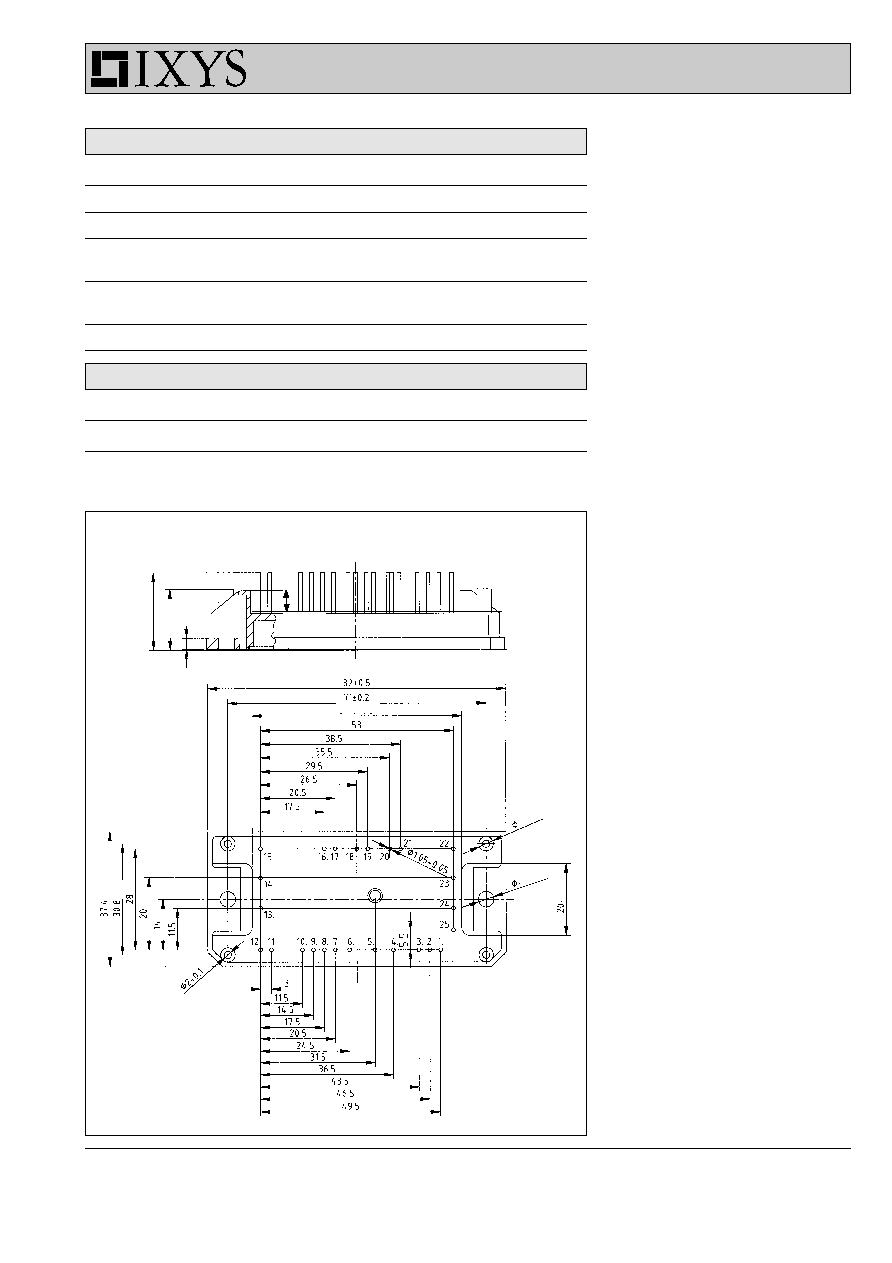
Dimensions in mm (1 mm = 0.0394")
21.1 ± 0.5
17.1 ± 0.3
3.4 ± 0.1
5.7 ± 0.3
57.3-0.3
5.5+0.2
4.3+0.2
© 2000 IXYS All rights reserved
5 - 8
MUBW 15-12 A6
D
6
D
)60
6
W
)
D
)
$
$
!
!$
!
"
#
$
%
$
$
!
!$
"
6
U
9-
√2√ "8
U
9-
√2√!$8
h
'√√W
550
$√C
U
9-
√2√#$8
U
9-
√2√ "8
W
U
9-
√2√#$8
U
9-
√2√ "8
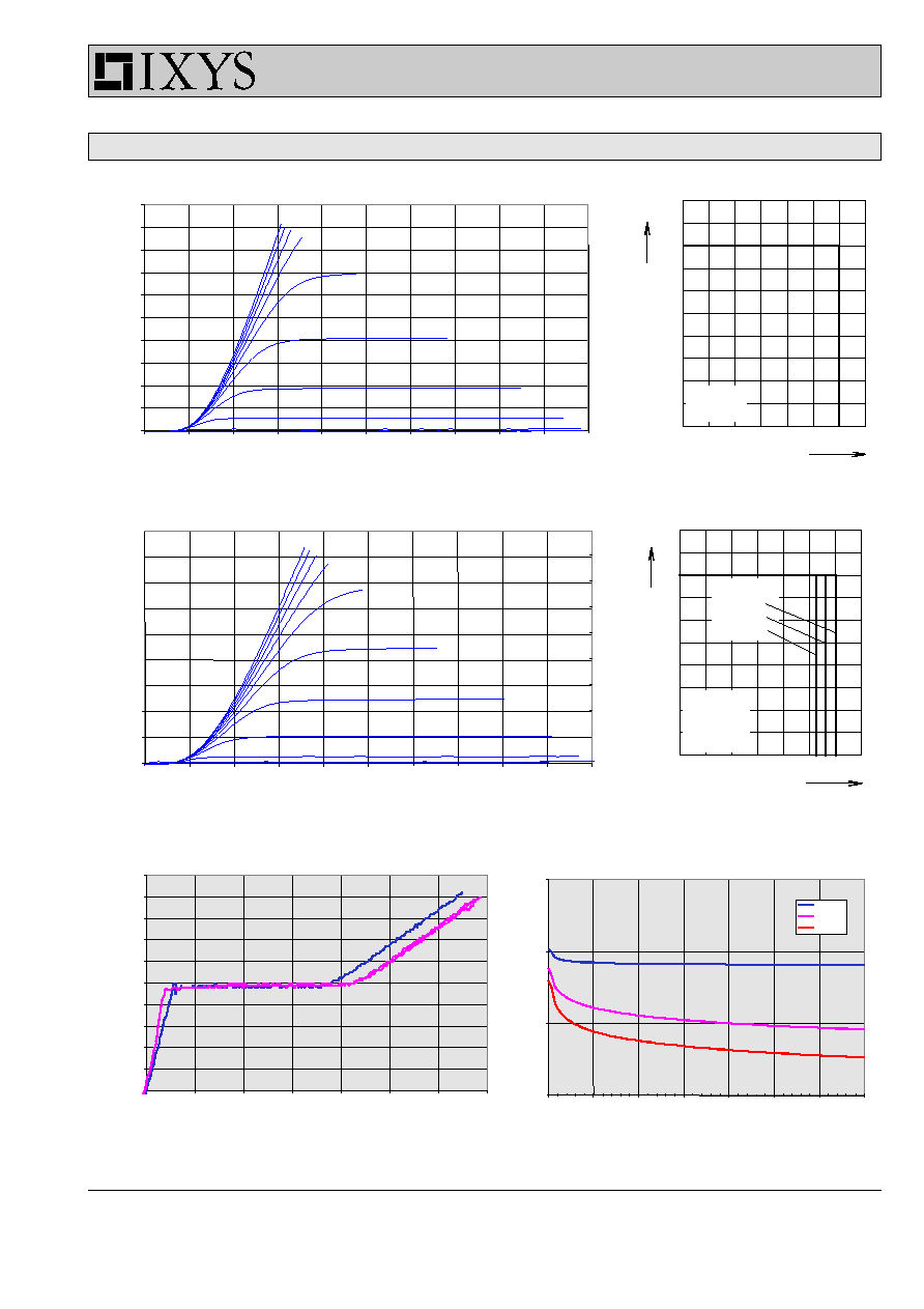
Forward characteristics
Surge overload current
I
FSM
: crest value, t: duration
I
2
t versus time (1-10 ms)
Z
thJH
[K/W]
0.0001
0.001
0.01
0.1
1
10
0.00001
0.0001
0.001
0.01
0.1
1
10
100
t (s)
D = 0
D = 0.005
D = 0.01
D = 0.02
D = 0.05
D = 0.1
D = 0.2
D = 0.5
Input Rectifier Bridge D8 - D13
(Z
thJH
is measured using 50 µm
thermal grease)
Transient thermal resistance junction to heatsink
© 2000 IXYS All rights reserved
6 - 8
MUBW 15-12 A6
U√√puhhprvvp√!$8
!
#
%
'
!
#
%
'
!
!
"
#
$
%
&
'
(
VprW
Dp6
h√i√p
q
r
s
t
u
v
w
x
VtW
h√√$W
i√√%W
p√√&W
q√√'W
r√√(W
s√√ W
t√ W
u√ !W
v√√ "W
w√√ #W
x√ $W
U√√puhhprvvp√ !$8
VprW
Dp6
DE
F
G
H
I
J
K
M
N
M
VtW
h√√$W
i√√%W
p√√&W
q√√'W
r√√(W
s√√ W
t√ W
u√ !W
v√√ "W
w√√ #W
x√ $W
√ √
!
#
%
'
!
#
%
'
!
!
"
#
$
%
&
8uhtr √8i
V
t
r
√
W
$
$
!
!$
"
"$
Vpr√W
8
√A
8v√A
8√A
8√A
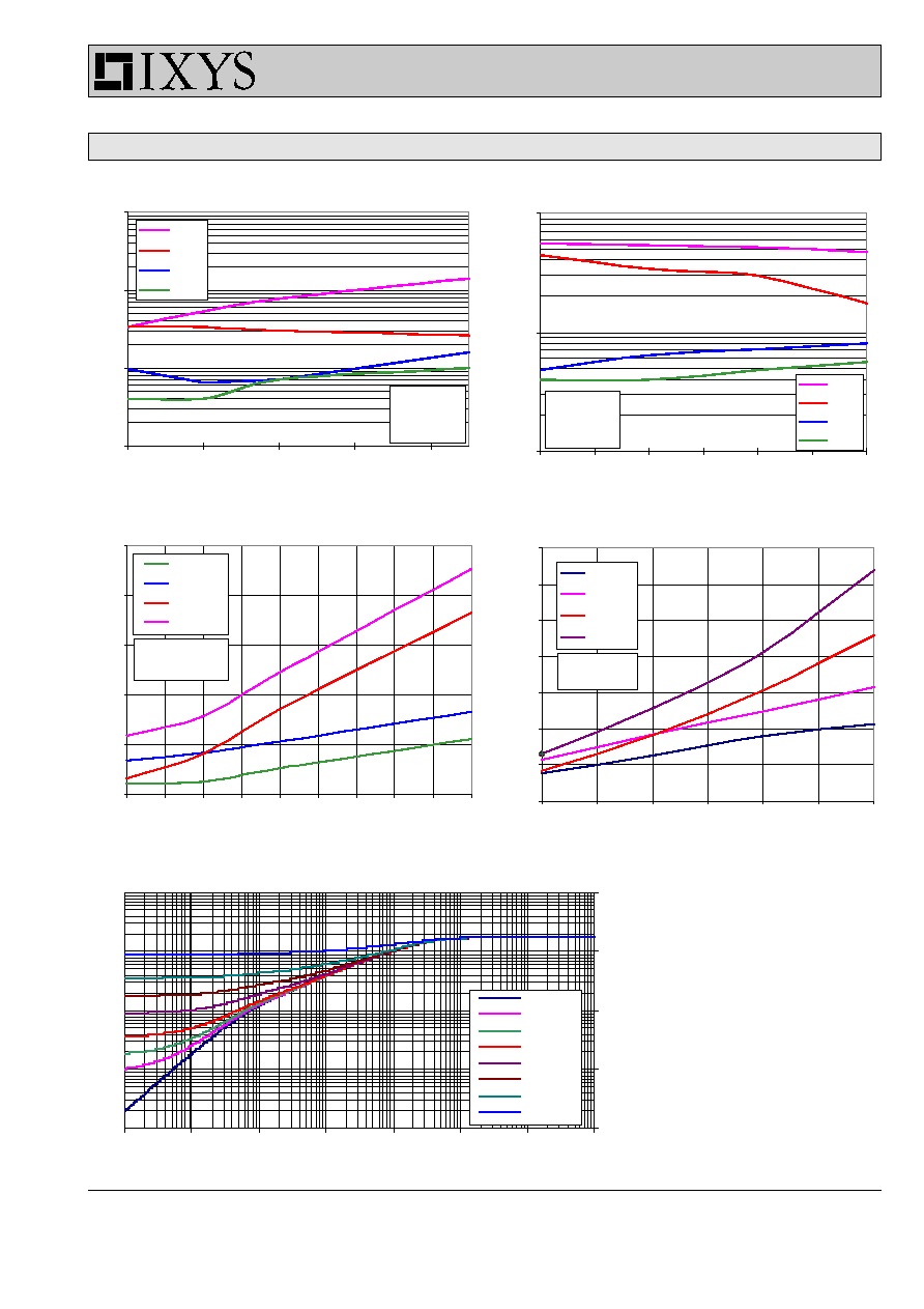
Output Inverter T1 - T6
0
400
800
1200
0.0
0.5
1.0
1.5
2.0
2.5
V
CE
I
Cpuls
/ I
C
V
T
V
J
= 150
∞
C
V
GE
= 15 V
Reverse biased safe operating area
0
400
800
1200
0
2
4
6
8
10
V
CE
I
Csc
/ I
C
V
T
V
J
= 150
∞
C
V
GE
= ±15 V
T
sc
£
10 µs
L < 50 nH
di/dt =
200 A/µs
600 A/µs
1000A/µs
Short circuit safe operating area
Typ. gate charge
Typ. capacitances
© 2000 IXYS All rights reserved
7 - 8
MUBW 15-12 A6
7\S VZLWFKLQJ WLPH
5J2KP�
W
Q
V
�
WGRII�
WIRII�
WGRQ�
WURQ�
U√vpuvt√yr√
St√Pu
(
P
:
V
�
(RII&�
(RII&�
(RQ&�
(RQ&�
Output Inverter T1 - T6
7\SVZLWFKLQJ WLPH
,$�
W
Q
V
�
WGRII�
WIRII�
WGRQ�
WURQ�
U√vpuvt√yr
,$�
(
P
:
V
�
(RII&�
(RII&�
(RQ&�
(RQ&�
,*%7
=WK- + >.:@
√
9√2√√√√
9√2√$
9√2√
9√2√!
9√2√$
9√2√ √
9√2√!√
9√2√$
Transient thermal resistance junction to heatsink
I
C
= 8 A
V
CE
= 600 V
T
VJ
= 125∞C
R
G
= 150
W
V
CE
= 600 V
T
VJ
= 125∞C
R
G
= 150
W
V
CE
= 600 V
I
C
= 8A
V
CE
= 600 V
(Z
thJH
is measured using 50 µm
thermal grease)
© 2000 IXYS All rights reserved
8 - 8
MUBW 15-12 A6
FRED
Z
thJH
[K/W]
0.001
0.01
0.1
1
10
0.00001
0.0001
0.001
0.01
0.1
1
10
100
t (s)
D = 0
D = 0.005
D = 0.01
D = 0.02
D = 0.05
D = 0.1
D = 0.2
D = 0.5
200
600
1000
0
400
800
100
120
140
160
180
0
40
80
120
160
0.0
0.5
1.0
1.5
2.0
K
f
T
VJ
∞C
-di
F
/dt
0
200
400
600
800
1000
0
40
80
120
0.0
0.4
0.8
1.2
V
FR
di
F
/dt
V
200
600
1000
0
400
800
0
10
20
30
40
50
100
1000
0.0
0.5
1.0
1.5
2.0
2.5
3.0
0
1
2
3
4
0
5
10
15
20
25
30
35
40
I
RM
Q
r
I
F
A
V
F
-di
F
/dt
-di
F
/dt
A/
m
s
A
V
m
C
A/
m
s
A/
m
s
t
rr
ns
t
fr
A/
m
s
m
s
I
F
= 30A
I
F
= 15A
I
F
= 7.5A
T
VJ
= 100∞C
V
R
= 600V
T
VJ
= 100∞C
I
F
= 15A
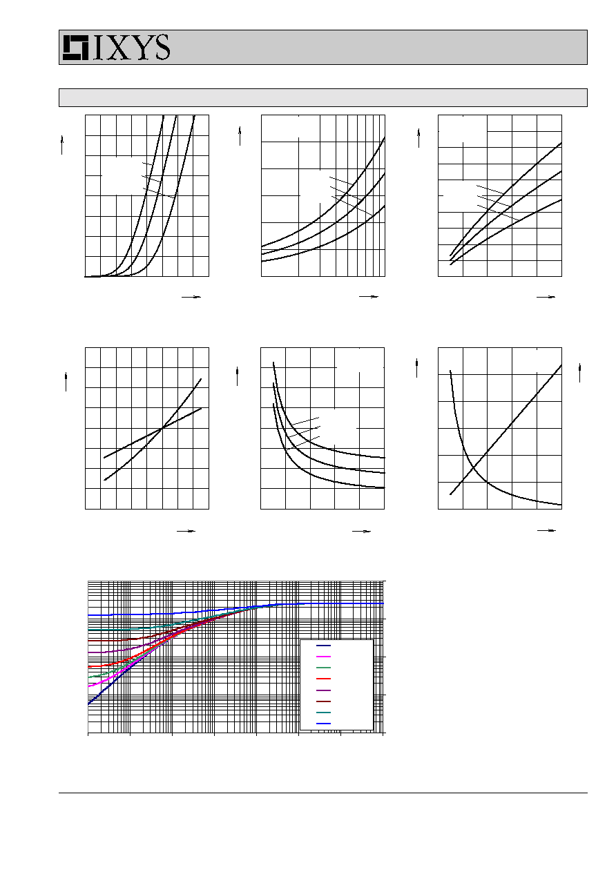
Peak reverse current I
RM
versus -di
F
/dt
Reverse recovery charge Q
r
versus -di
F
/dt
Forward current I
F
versus V
F
T
VJ
= 100∞C
V
R
= 600V
T
VJ
= 100∞C
V
R
= 600V
I
F
= 30A
I
F
= 15A
I
F
= 7.5A
Q
r
I
RM
Dynamic parameters Q
r
, I
RM
versus T
VJ
Recovery time t
rr
versus -di
F
/dt
Peak forward voltage V
FR
and t
fr
versus di
F
/dt
I
F
= 30A
I
F
= 15A
I
F
= 7.5A
t
fr
V
FR
T
VJ
=150∞C
T
VJ
=100∞C
T
VJ
= 25∞C
Output Inverter D1 - D6
15-12A
Transient thermal resistance junction to heatsink
(Z
thJH
is measured using 50 µm
thermal grease)