
© 2000 IXYS All rights reserved
1 - 4
023
IXYS reserves the right to change limits, test conditions and dimensions.
IXYS reserves the right to change limits, test conditions and dimensions.
Features
q
NPT IGBT technology
q
low saturation voltage
q
low switching losses
q
switching frequency up to 30 kHz
q
square RBSOA, no latch up
q
high short circuit capability
q
positive temperature coefficient for
easy parallelling
q
MOS input, voltage controlled
q
ultra fast free wheeling diodes
q
solderable pins for PCB mounting
q
package with copper base plate
Advantages
q
space savings
q
reduced protection circuits
q
package designed for wave soldering
Typical Applications
q
AC motor control
q
AC servo and robot drives
q
power supplies
IGBTs
Symbol
Conditions
Maximum Ratings
V
CES
T
VJ
= 25∞C to 150∞C
600
V
V
GES
±
20
V
I
C25
T
C
= 25∞C
72
A
I
C80
T
C
= 80∞C
50
A
RBSOA
V
GE
=
±
15 V; R
G
= 22
W
; T
VJ
= 125∞C
I
CM
= 100
A
Clamped inductive load; L = 100 µH
V
CEK
£
V
CES
t
SC
V
CE
= V
CES
; V
GE
=
±
15 V; R
G
= 22
W
; T
VJ
= 125∞C
10
µs
(SCSOA)
non-repetitive
P
tot
T
C
= 25∞C
225
W
Symbol
Conditions
Characteristic Values
(T
VJ
= 25
∞
C, unless otherwise specified)
min.
typ.
max.
V
CE(sat)
I
C
= 50 A; V
GE
= 15 V; T
VJ
= 25∞C
1.9
2.4
V
T
VJ
= 125∞C
2.2
V
V
GE(th)
I
C
= 1 mA; V
GE
= V
CE
4.5
6.5
V
I
CES
V
CE
= V
CES
;
V
GE
= 0 V; T
VJ
= 25∞C
0.6
mA
T
VJ
= 125∞C
0.7
mA
I
GES
V
CE
= 0 V; V
GE
=
±
20 V
200
nA
t
d(on)
50
ns
t
r
60
ns
t
d(off)
300
ns
t
f
30
ns
E
on
2.3
mJ
E
off
1.7
mJ
C
ies
V
CE
= 25 V; V
GE
= 0 V; f = 1 MHz
2800
pF
Q
Gon
V
CE
= 300V; V
GE
= 15 V; I
C
= 50 A
120
nC
R
thJC
(per IGBT)
0.55 K/W
Inductive load, T
VJ
= 125∞C
V
CE
= 300 V; I
C
= 50 A
V
GE
= ±15 V; R
G
= 22
W
I
C25
= 72 A
V
CES
= 600 V
V
CE(sat) typ.
= 1.9 V
IGBT Modules
Sixpack
Short Circuit SOA Capability
Square RBSOA
Type:
NTC - Option:
MWI 50-06 A7
without NTC
MWI 50-06 A7T
with NTC
NTC
13
17
1
2
3
4
7
8
9
10
11
12
5
6
15
16
14
T
T
MWI 50-06 A7
MWI 50-06 A7T
Preliminary Data
© 2000 IXYS All rights reserved
2 - 4
Diodes
Symbol
Conditions
Maximum Ratings
I
F25
T
C
= 25∞C
72
A
I
F80
T
C
= 80∞C
45
A
Symbol
Conditions
Characteristic Values
min.
typ.
max.
V
F
I
F
= 50 A; V
GE
= 0 V; T
VJ
= 25∞C
1.6
1.8
V
T
VJ
= 125∞C
1.3
1.5
V
I
RM
I
F
= 30 A; di
F
/dt = -500 A/µs; T
VJ
= 125∞C
25
A
t
rr
V
R
= 300 V; V
GE
= 0 V
90
ns
R
thJC
(per diode)
1.19 K/W
Temperature Sensor NTC (MWI ... A7T version only)
Symbol
Conditions
Characteristic Values
min.
typ.
max.
R
25
T = 25∞C
4.75
5.0
5.25
k
W
B
25/50
3375
K
Module
Symbol
Conditions
Maximum Ratings
T
VJ
-40...+150
∞
C
T
stg
-40...+125
∞
C
V
ISOL
I
ISOL
£
1 mA; 50/60 Hz
2500
V~
M
d
Mounting torque (M5)
2.7 - 3.3
Nm
Symbol
Conditions
Characteristic Values
min.
typ.
max.
R
pin-chip
5
m
W
d
S
Creepage distance on surface
6
mm
d
A
Strike distance in air
6
mm
R
thCH
with heatsink compound
0.02
K/W
Weight
180
g
MWI 50-06 A7
MWI 50-06 A7T
Dimensions in mm (1 mm = 0.0394")
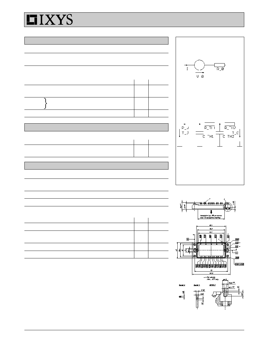
Equivalent Circuits for Simulation
Conduction
IGBT (typ. at V
GE
= 15 V; T
J
= 125∞C)
V
0
= 0.82 V; R
0
= 28 mW
Free Wheeling Diode (typ. at T
J
= 125∞C)
V
0
= 0.89 V; R
0
= 8 mW
Thermal Response
IGBT (typ.)
C
th1
= 0.201 J/K; R
th1
= 0.42 K/W
C
th2
= 1.252 J/K; R
th2
= 0.131K/W
Free Wheeling Diode (typ.)
C
th1
= 0.116 J/K; R
th1
= 0.973 K/W
C
th2
= 0.88 J/K; R
th2
= 0.217 K/W
Higher magnification see outlines.pdf

© 2000 IXYS All rights reserved
3 - 4
MWI 50-06 A7
MWI 50-06 A7T
0
200
400
600
800
1000
0
10
20
30
40
50
0
30
60
90
120
150
0
1
2
3
4
5
6
0
30
60
90
120
150
0
40
80
120
160
0
5
10
15
20
0
1
2
3
4
5
6
0
30
60
90
120
150
T
VJ
= 25∞C
T
VJ
= 125∞C
V
CE
= 300V
I
C
= 50A
V
CE
V
I
C
V
CE
A
I
C
V
nC
Q
G
-di/dt
V
V
GE
I
RM
t
rr
A/
m
s
MWI5006A7
T
VJ
= 125∞C
V
R
= 300V
I
F
= 30A
I
RM
t
rr
9V
11V
V
GE
= 17V
15V
13V
A
9V
11V
V
GE
= 17V
15V
13V
A
4
6
8
10
12
14
16
0
30
60
90
120
150
V
CE
= 20V
V
V
GE
A
I
C
T
VJ
= 25∞C
T
VJ
= 125∞C
0.0
0.5
1.0
1.5
2.0
0
15
30
45
60
75
90
V
V
F
I
F
T
VJ
= 25∞C
T
VJ
= 125∞C
A
ns
Fig. 1
Typ. output characteristics
Fig. 2 Typ. output characteristics
Fig. 3
Typ. transfer characteristics
Fig. 4 Typ. forward characteristics of
free wheeling diode
Fig. 5
Typ. turn on gate charge
Fig. 6 Typ. turn off characteristics of
free wheeling diode

© 2000 IXYS All rights reserved
4 - 4
MWI 50-06 A7
MWI 50-06 A7T
Fig. 7
Typ. turn on energy and switching
Fig. 8 Typ. turn off energy and switching
times versus collector current
times versus collector current
Fig. 9
Typ. turn on energy and switching
Fig.10 Typ. turn off energy and switching
times versus gate resistor
times versus gate resistor
Fig. 11 Reverse biased safe operating area
Fig. 12 Typ. transient thermal impedance
RBSOA
0
40
80
120
0.0
2.5
5.0
7.5
10.0
0
25
50
75
100
0
40
80
120
0
1
2
3
4
0
100
200
300
400
0.00001 0.0001 0.001
0.01
0.1
1
10
0.0001
0.001
0.01
0.1
1
10
0
10
20
30
40
50
60
0
1
2
3
0
200
400
600
0
10
20
30
40
50
60
1
2
3
4
20
40
60
80
single pulse
V
CE
= 300V
V
GE
= ±15V
R
G
= 22
W
T
VJ
= 125∞C
MWI5006A7
V
CE
= 300V
V
GE
= ±15V
I
C
= 50A
T
VJ
= 125∞C
0
100
200
300
400
500
600
700
0
30
60
90
120
R
G
= 22
W
T
VJ
= 125∞C
V
CE
= 300V
V
GE
= ±15V
R
G
= 22
W
T
VJ
= 125∞C
E
on
V
CE
= 300V
V
GE
= ±15V
I
C
= 50A
T
VJ
= 125∞C
t
d(on)
t
r
E
off
t
d(off)
t
f
E
on
t
d(on)
t
r
E
off
t
d(off)
t
f
I
C
A
I
C
A
E
off
E
on
t
t
R
G
W
R
G
W
V
CE
t
s
mJ
E
on
mJ
E
off
ns
t
ns
t
I
CM
K/W
Z
thJC
IGBT
diode
V
A
mJ
ns
ns
mJ