Rev. 1.0 - 5/01/98
1
PRELIMINARY
1
2
3
4
5
6
7
8
9
10
11
12
PDM21532
Description
The PDM21532 is a high-performance CMOS static
RAM organized as 65,536 x 16 bits. The PDM21532
features low power dissipation using chip enable
(CE) and has an output enable input (OE) for fast
memory access. Byte access is supported by upper
and lower byte controls.
The PDM21532 operates from a single 2.7V power
supply and all inputs and outputs are fully TTL-
compatible.
The PDM21532 is available in a 44-pin 400-mil plas-
tic SOJ and a plastic TSOP (II) package for high-
density surface assembly and is suitable for use in
high-speed applications requiring high-speed
storage.
PDM21532
64K x 16 CMOS
2.7V Static RAM
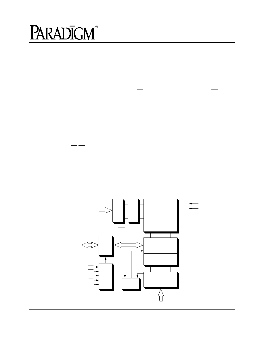
A8-A0
Memory
Cell
Array
256 x 128 x 32
Row Address
Buffer
Control
Logic
Sense Amp
Column
Decoder
Column
Address
Buffer
Row Decoder
Clock
Generator
A15-A9
CE
LB
UB
OE
WE
Data
Input/
Output
Buffer
Vcc
Vss
I/O15-I/O0
Features
n
High-speed access times
- Com'l: 70, 85 and 100 ns
- Ind: 85 and 100 ns
n
Low power operation (typical)
- PDM21532LA
Active: 100 mW
Standby: 150
µ
W
n
High-density 64K x 16 architecture
n
2.7V (
±
0.2V) power supply
n
Fully static operation
n
TTL-compatible inputs and outputs
n
Output buffer controls: OE
n
Data byte controls: LB, UB
n
Packages:
Plastic SOJ (400 mil) - SO
Plastic TSOP (II) - T
Functional Block Diagram
32K x 32

PDM21532
Rev. 1.0 - 5/01/98
3
PRELIMINARY
1
2
3
4
5
6
7
8
9
10
11
12
Operating Mode
NOTE: 1. H = V
IH
, L = V
IL
, X = DON'T CARE
Mode
CE
OE
WE
LB
UB
I/O7-I/O0
I/O15-I/O8
Power
Read
L
L
H
L
L
Output
Output
I
CC
H
L
High Impedance
Output
I
CC
L
H
Output
High Impedance
I
CC
Write
L
X
L
L
L
Input
Input
I
CC
H
L
High Impedance
Input
I
CC
L
H
Input
High Impedance
I
CC
Output Disable
L
H
H
X
x
High Impedance
High Impedance
I
CC
L
X
X
H
H
High Impedance
High Impedance
I
CC
Standby
H
X
X
X
X
High Impedance
High Impedance
I
SB
Absolute Maximum Ratings
(1)
NOTE: 1. Stresses greater than those listed under ABSOLUTE MAXIMUM RATINGS may
cause permanent damage to the device. This is a stress rating only and functional
operation of the device at these or any other conditions above those indicated in the
operational sections of this specification is not implied. Exposure to absolute maxi-
mum rating conditions for extended periods may affect reliability.
2. Appropriate thermal calculations should be performed in all cases and specifically for
those where the chosen package has a large thermal resistance (e.g., TSOP). The
calculation should be of the form
: T
j
= T
a
+ P *
ja
where T
a
is the ambient tempera-
ture, P is average operating power and
ja
the thermal resistance of the package. For
this product, use the following
ja
values:
SOJ: 59
o
C/W
TSOP: 87
o
C/W
Recommended DC Operating Conditions
Symbol
Rating
Com'l.
Ind.
Unit
V
TERM
Terminal Voltage with Respect to V
SS
≠0.5 to +4.6
≠0.5 to +4.6
V
T
BIAS
Temperature Under Bias
≠55 to +125
≠65 to +135
∞
C
T
STG
Storage Temperature
≠55 to +125
≠65 to +150
∞
C
P
T
Power Dissipation
0.8
0.8
W
I
OUT
DC Output Current
50
50
mA
T
j
Maximum Junction Temperature
(2)
125
125
∞
C
Symbol
Description
Min.
Typ.
Max.
Unit
V
CC
Supply Voltage
2.5
2.7
2.9
V
V
SS
Supply Voltage
0
0
0
V
Industrial
Ambient Temperature
≠40
25
85
∞
C
Commercial
Ambient Temperature
0
25
70
∞
C

PDM21532
4
Rev. 1.0 - 5/01/98
PRELIMINARY
Power Supply Characteristics
NOTES: All values are maximum guaranteed values.
-70
-85
-100
Symbol Parameter
Com'l Com'l
Ind.
Com'l
Ind.
Unit
I
CC
Operating Current
CE = V
IL
f = f
MAX
= 1/t
RC
V
CC
= Max.
I
OUT
= 0 mA
LA
55
45
50
40
45
mA
I
SB1
Full Standby Cur-
rent
CE
V
CC
≠ 0.2V
LA
800
800
850
750
800
µ
A
f = 0
V
CC
= Max.,
V
IN
V
CC
≠ 0.2V
or
0.2V
DC Electrical Characteristics
(V
CC
= 2.7V
±
0.2V)
NOTE: 1.V
IL
(min) = ≠0.3V for pulse width less than 30 ns.
Symbol
Parameter
Test Conditions
Min.
Max.
Unit
I
LI
Input Leakage Current
V
CC
= Max., V
IN
= Vss to V
CC
≠1
1
µ
A
I
LO
Output Leakage Current
V
CC
= Max.,
CE = V
IH
, V
OUT
= Vss to V
CC
≠1
1
µ
A
V
IL
Input Low Voltage
≠0.3
(1)
0.4
V
V
IH
Input High Voltage
2.2
Vcc +
0.3
V
V
OL
Output Low Voltage
I
OL
= 2.1mA, V
CC
= Min.
--
0.4
V
V
OH
Output High Voltage
I
OH
= ≠1.0 mA, V
CC
= Min.
2.2
--
V
PDM21532
Rev. 1.0 - 5/01/98
5
PRELIMINARY
1
2
3
4
5
6
7
8
9
10
11
12
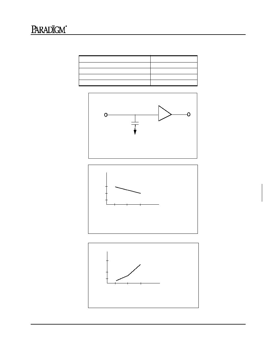
CL *
AC Test Conditions
Input pulse levels
V
ss
to V
cc
Input rise and fall times
5.0 NS
Input timing reference levels
1.5V
Output reference levels
1.5V
Output load
See Figures 1 and 2
40
20
30
-45
25
Temperature in
∞
C
I
CC
in mA
-45
25
80
∑
∑
∑
40
35
30
1000
10
100
-45
25
80
I
SB1
in
µ
A
Temperature in
∞
C
∑
∑
∑
10
50
750
Figure 3.
I
SB1
vs. Ambient Temperature (V
CC
= V
CC
Max.)
Figure 2.
I
CC
vs. Ambient Temperature (V
CC
= V
CC
Max.)
Figure 1.
Output Load (* includes scope and JIG capacitance)
Typically = 100pF
