Document Outline
- Pin Configuration
- VTERM
- Terminal Voltage with Respect to VSS
- Ö0.5 to +4.6
- Ö0.5 to +4.6
- V
- TBIAS
- Temperature Under Bias
- Ö55 to +125
- Ö65 to +135
- ∞C
- TSTG
- Storage Temperature
- Ö55 to +125
- Ö65 to +150
- ∞C
- PT
- Power Dissipation
- 1.5
- 1.5
- W
- IOUT
- DC Output Current
- 50
- 50
- mA
- Tj
- Maximum Junction Temperature (3)
- 125
- 145
- ∞C
- VCC
- Supply Voltage
- 3.0
- 3.3
- 3.6
- V
- VSS
- Supply Voltage
- 0
- 0
- 0
- V
- Industrial
- Ambient Temperature
- Ö40
- 25
- 85
- ∞C
- Commercial
- Ambient Temperature
- 0
- 25
- 70
- ∞C
- ICC
- Operating Current
- CE = VIL
- SA
- 175
- 165
- 150
- 160
- 130
- 140
- 120
- 130
- mA
- f = fMAX = 1/tRC
- VCC = Max.
- IOUT = 0 mA
- LA
- 150
- 140
- 130
- 140
- 120
- 130
- 110
- 120
- mA
- ISB
- Standby Current
- CE = VIH
- SA
- 30
- 30
- 30
- 30
- 30
- 30
- 30
- 30
- mA
- f = fMAX = 1/tRC
- VCC = Max.
- LA
- 15
- 15
- 15
- 15
- 15
- 15
- 15
- 15
- mA
- ISB1
- Full Standby
- Current
- CE ≥ VCC Ö 0.2V
- SA
- 5
- 5
- 5
- 5
- 5
- 5
- 5
- 5
- mA
- f = 0
- VCC = Max.,
- VIN ≥ VCC Ö 0.2V or £ 0.2V
- LA
- 2
- 2
- 2
- 5
- 2
- 5
- 2
- 5
- mA
- Features
- n High-speed access times - Comêl: 9, 10, 12, 15 a...
- n Low power operation (typical) - PDM31532LA Activ...
- - PDM31532SA Active: 250 mW Standby: 20 mW
- n High-density 64K x 16 architecture
- n 3.3V (±0.3V) power supply
- n Fully static operation
- n TTL-compatible inputs and outputs
- n Output buffer controls: OE
- n Data byte controls: LB, UB
- n Packages:
- Plastic SOJ (400 mil) - SO Plastic TSOP - T (II)
- SOJ
- Read
- L
- L
- H
- L
- L
- Output
- Output
- ICC
- H
- L
- High Impedance
- Output
- ICC
- L
- H
- Output
- High Impedance
- ICC
- Write
- L
- X
- L
- L
- L
- Input
- Input
- ICC
- H
- L
- High Impedance
- Input
- ICC
- L
- H
- Input
- High Impedance
- ICC
- Output Disable
- L
- H
- H
- X
- x
- High Impedance
- High Impedance
- ICC
- L
- X
- X
- H
- H
- High Impedance
- High Impedance
- ICC
- Standby
- H
- X
- X
- X
- X
- High Impedance
- High Impedance
- ISB
- WRITE cycle time
- tWC
- 9
- Ñ
- 10
- Ñ
- 12
- Ñ
- 15
- Ñ
- 20
- Ñ
- ns
- Chip enable to end of write
- tCW
- 8
- Ñ
- 9
- Ñ
- 10
- Ñ
- 11
- Ñ
- 12
- Ñ
- ns
- Address valid to end of write
- tAW
- 8
- Ñ
- 9
- Ñ
- 10
- Ñ
- 11
- Ñ
- 12
- Ñ
- ns
- Byte pulse width
- tBW
- 8
- Ñ
- 9
- Ñ
- 10
- Ñ
- 12
- Ñ
- 13
- Ñ
- ns
- Address setup time
- tAS
- 0
- Ñ
- 0
- Ñ
- 0
- Ñ
- 0
- Ñ
- 0
- Ñ
- ns
- Address hold from end of write
- tAH
- 0
- Ñ
- 0
- Ñ
- 0
- Ñ
- 0
- Ñ
- 0
- Ñ
- ns
- Write pulse width
- tWP
- 7
- Ñ
- 7
- Ñ
- 8
- Ñ
- 9
- Ñ
- 10
- Ñ
- ns
- Data setup time
- tDS
- 6
- Ñ
- 6
- Ñ
- 7
- Ñ
- 8
- Ñ
- 9
- Ñ
- ns
- Data hold time
- tDH
- 0
- Ñ
- 0
- Ñ
- 0
- Ñ
- 0
- Ñ
- 0
- Ñ
- ns
- Byte disable to output in low Z(1, 5, 8)
- tLZBE
- 1
- Ñ
- 1
- Ñ
- 1
- Ñ
- 1
- Ñ
- 1
- Ñ
- ns
- Byte enable to output in high Z(1, 5, 8)
- tHZBE
- Ñ
- 7
- Ñ
- 7
- Ñ
- 7
- Ñ
- 8
- Ñ
- 9
- ns
- Output disable to output in low Z(1, 5, 8)
- tLZOE
- 0
- Ñ
- 0
- Ñ
- 0
- Ñ
- 0
- Ñ
- 0
- Ñ
- ns
- Output enable to output in high Z(1, 5, 8)
- tHZOE
- Ñ
- 7
- Ñ
- 7
- Ñ
- 7
- Ñ
- 8
- Ñ
- 9
- ns
- Write disable to output in low Z(1, 5, 8)
- tLZWE
- 1
- Ñ
- 1
- Ñ
- 1
- Ñ
- 1
- Ñ
- 1
- Ñ
- ns
- Write enable to output in high Z(1, 5, 8)
- tHZWE
- Ñ
- 7
- Ñ
- 7
- Ñ
- 7
- Ñ
- 8
- Ñ
- 9
- ns
- Ordering Information
- READ cycle time
- tRC
- 9
- Ñ
- 10
- Ñ
- 12
- Ñ
- 15
- Ñ
- 20
- Ñ
- ns
- Address access time
- tAA
- Ñ
- 9
- Ñ
- 10
- Ñ
- 12
- Ñ
- 15
- Ñ
- 20
- ns
- Chip enable access time
- tACE
- Ñ
- 9
- Ñ
- 10
- Ñ
- 12
- Ñ
- 15
- Ñ
- 20
- ns
- Byte access time
- tBA
- Ñ
- 6
- Ñ
- 6
- Ñ
- 7
- Ñ
- 8
- Ñ
- 9
- ns
- Output hold from address change
- tOH
- 3
- Ñ
- 3
- Ñ
- 3
- Ñ
- 3
- Ñ
- 3
- Ñ
- ns
- Byte disable to output in low-Z
- tLZBE
- 0
- Ñ
- 0
- Ñ
- 0
- Ñ
- 0
- Ñ
- 0
- Ñ
- ns
- Byte enable to output in high-Z
- tHZBE
- Ñ
- 7
- Ñ
- 7
- Ñ
- 8
- Ñ
- 9
- Ñ
- 9
- ns
- Chip enable to output in low-Z(1, 5)
- tLZCE
- 3
- Ñ
- 3
- Ñ
- 3
- Ñ
- 3
- Ñ
- 3
- Ñ
- ns
- Chip disable to output high-Z(1, 5)
- tHZCE
- Ñ
- 6
- Ñ
- 6
- Ñ
- 7
- Ñ
- 8
- Ñ
- 9
- ns
- Output enable access time
- tAOE
- Ñ
- 6
- Ñ
- 6
- Ñ
- 7
- Ñ
- 8
- Ñ
- 9
- ns
- Output enable to output in low-Z(1, 5)
- tLZOE
- 0
- Ñ
- 0
- Ñ
- 0
- Ñ
- 0
- Ñ
- 0
- Ñ
- ns
- Output disable to output in high-Z(1, 5)
- tHZOE
- Ñ
- 6
- Ñ
- 6
- Ñ
- 7
- Ñ
- 8
- Ñ
- 9
- ns
- ILI
- Input Leakage Current
- VCC = Max., VIN = Vss to VCC
- Comêl/
- Ind.
- Ö5
- 5
- mA
- ILO
- Output Leakage Current
- VCC= Max.,
- CE = VIH, VOUT = Vss to VCC
- Comêl/
- Ind.
- Ö5
- 5
- mA
- VIL
- Input Low Voltage
- Ö0.3(4)
- 0.8
- V
- VIH
- Input High Voltage
- 2.2
- Vcc + 0.3
- V
- VOL
- Output Low Voltage
- IOL = 8 mA, VCC = Min.
- Ñ
- 0.4
- V
- VOH
- Output High Voltage
- IOH = Ö4 mA, VCC = Min.
- 2.4
- Ñ
- V
- CIN
- Input Capacitance
- VIN = VSS
- 6
- pF
- CI/O
- Output Capacitance
- VI/O = VSS
- 8
- pF
- A15-A0
- Address Inputs
- I/O15-I/O0
- Data Inputs
- CE
- Chip Enable Input
- WE
- Write Enable Input
- OE
- Output Enable Input
- LB, UB
- Data Byte Control Inputs
- NC
- No Connect
- Vss
- Ground
- VCC
- Power (+3.3V)
- TSOP (II)
- Write Cycle 1 Timing Diagram(8) (WE Controlled)
- Write Cycle 2 Timing Diagram(8) (CE Controlled)
- Input pulse levels
- VSS to 3.0V
- Input rise and fall times
- 2.5 NS
- Input timing reference levels
- 1.5V
- Output reference levels
- 1.5V
- Output load
- See Figures 1 and 2
- Write Cycle 3 Timing Diagram(8) (UB, LB Controlled...
- PDM31532
- 64K x 16 CMOS
- 3.3V Static RAM
- Read Timing Diagram
Rev. 4.3 - 3/27/98
1
1
2
3
4
5
6
7
8
9
10
11
12
PDM31532
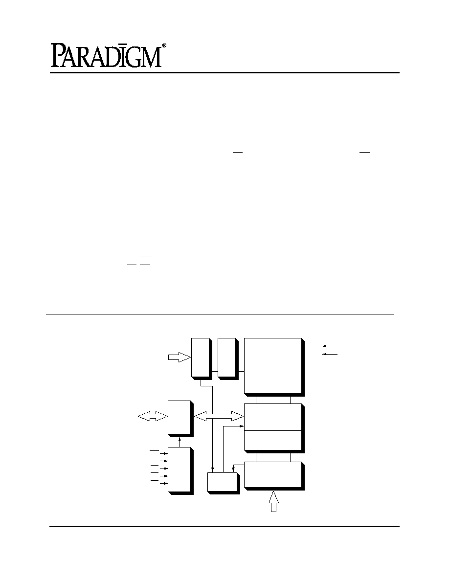
Description
The PDM31532 is a high-performance CMOS static
RAM organized as 65,536 x 16 bits. The PDM31532
features low power dissipation using chip enable
(CE) and has an output enable input (OE) for fast
memory access. Byte access is supported by upper
and lower byte controls.
The PDM31532 operates from a single 3.3V power
supply and all inputs and outputs are fully TTL-
compatible.
The PDM31532 is available in a 44-pin 400 mil plas-
tic SOJ and a plastic TSOP (II) package for high-
density surface assembly and is suitable for use in
high-speed applications requiring high-speed
storage.
PDM31532
64K x 16 CMOS
3.3V Static RAM
A8-A0
Memory
Cell
Array
256 x 128 x 32
Row Address
Buffer
Control
Logic
Sense Amp
Column
Decoder
Column
Address
Buffer
Row Decoder
Clock
Generator
A15-A9
CE
LB
UB
OE
WE
Data
Input/
Output
Buffer
Vcc
Vss
I/O15-I/O0
Features
n
High-speed access times
- Com'l: 9, 10, 12, 15 and 20 ns
- Ind: 12, 15 and 20 ns
n
Low power operation (typical)
- PDM31532LA
Active: 200 mW
Standby: 10 mW
- PDM31532SA
Active: 250 mW
Standby: 20 mW
n
High-density 64K x 16 architecture
n
3.3V (
±
0.3V) power supply
n
Fully static operation
n
TTL-compatible inputs and outputs
n
Output buffer controls: OE
n
Data byte controls: LB, UB
n
Packages:
Plastic SOJ (400 mil) - SO
Plastic TSOP - T (II)
Functional Block Diagram
32K x 32
PDM31532
2
Rev. 4.3 - 3/27/98
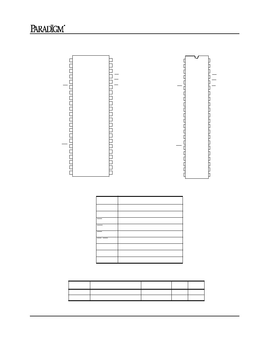
Pin Configuration
SOJ
Capacitance
(1)
(T
A
= +25
∞
C, f = 1.0 MHz)
NOTE: 1. This parameter is determined by device characterization, but is not production tested.
Symbol
Parameter
Conditions
Max.
Unit
C
IN
Input Capacitance
V
IN
= V
SS
6
pF
C
I/O
Output Capacitance
V
I/O
= V
SS
8
pF
1
2
3
4
5
6
7
8
9
10
11
12
15
16
29
30
31
32
A4
A3
A2
A1
A0
CE
I/O0
I/O1
I/O2
I/O3
Vcc
Vss
I/O4
I/O5
I/O6
I/O7
WE
A15
A14
A13
A12
NC
A5
A6
A7
OE
UB
LB
I/O15
I/O14
I/O13
I/O12
Vss
Vcc
I/O11
I/O10
I/O9
I/O8
NC
A8
A9
A10
A11
NC
13
14
33
34
35
36
37
38
39
40
41
42
43
44
19
20
21
22
17
18
23
24
25
26
27
28
Pin Description
Name
Description
A15-A0
Address Inputs
I/O15-I/O0
Data Inputs
CE
Chip Enable Input
WE
Write Enable Input
OE
Output Enable Input
LB, UB
Data Byte Control Inputs
NC
No Connect
V
ss
Ground
V
CC
Power (+3.3V)
1
2
3
4
5
6
7
8
9
10
11
12
15
16
29
30
31
32
A4
A3
A2
A1
A0
CE
I/O0
I/O1
I/O2
I/O3
Vcc
Vss
I/O4
I/O5
I/O6
I/O7
WE
A15
A14
A13
A12
NC
A5
A6
A7
OE
UB
LB
I/O15
I/O14
I/O13
I/O12
Vss
Vcc
I/O11
I/O10
I/O9
I/O8
NC
A8
A9
A10
A11
NC
13
14
33
34
35
36
37
38
39
40
41
42
43
44
19
20
21
22
17
18
23
24
25
26
27
28
TSOP (II)
PDM31532
Rev. 4.3 - 3/27/98
3
1
2
3
4
5
6
7
8
9
10
11
12
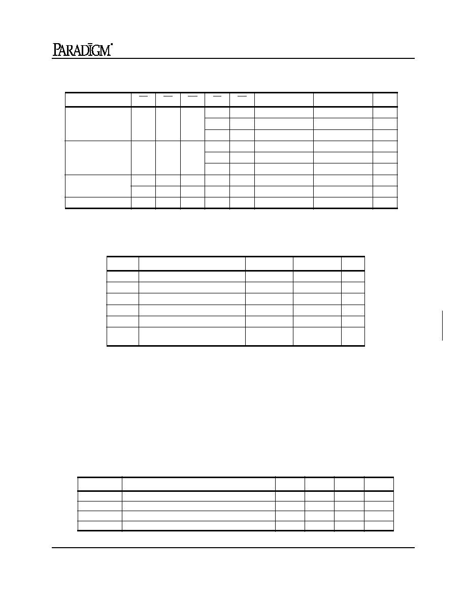
Operating Mode
NOTE:
H = V
IH
, L = V
IL
, X = DON'T CARE
Mode
CE
OE
WE
LB
UB
I/O7-I/O0
I/O15-I/O8
Power
Read
L
L
H
L
L
Output
Output
I
CC
H
L
High Impedance
Output
I
CC
L
H
Output
High Impedance
I
CC
Write
L
X
L
L
L
Input
Input
I
CC
H
L
High Impedance
Input
I
CC
L
H
Input
High Impedance
I
CC
Output Disable
L
H
H
X
x
High Impedance
High Impedance
I
CC
L
X
X
H
H
High Impedance
High Impedance
I
CC
Standby
H
X
X
X
X
High Impedance
High Impedance
I
SB
Absolute Maximum Ratings
(2)
NOTE: 2. Stresses greater than those listed under ABSOLUTE MAXIMUM RATINGS may
cause permanent damage to the device. This is a stress rating only and functional
operation of the device at these or any other conditions above those indicated in the
operational sections of this specification is not implied. Exposure to absolute maxi-
mum rating conditions for extended periods may affect reliability.
3. Appropriate thermal calculations should be performed in all cases and specifically for
those where the chosen package has a large thermal resistance (e.g., TSOP). The
calculation should be of the form
: T
j
= T
a
+ P *
ja
where T
a
is the ambient tempera-
ture, P is average operating power and
ja
the thermal resistance of the package. For
this product, use the following
ja
values:
SOJ: 59
o
C/W
TSOP: 87
o
C/W
Recommended DC Operating Conditions
Symbol
Rating
Com'l.
Ind.
Unit
V
TERM
Terminal Voltage with Respect to V
SS
≠0.5 to +4.6
≠0.5 to +4.6
V
T
BIAS
Temperature Under Bias
≠55 to +125
≠65 to +135
∞
C
T
STG
Storage Temperature
≠55 to +125
≠65 to +150
∞
C
P
T
Power Dissipation
1.5
1.5
W
I
OUT
DC Output Current
50
50
mA
T
j
Maximum Junction Temperature
(3)
125
145
∞
C
Symbol
Description
Min.
Typ.
Max.
Unit
V
CC
Supply Voltage
3.0
3.3
3.6
V
V
SS
Supply Voltage
0
0
0
V
Industrial
Ambient Temperature
≠40
25
85
∞
C
Commercial
Ambient Temperature
0
25
70
∞
C
PDM31532
4
Rev. 4.3 - 3/27/98
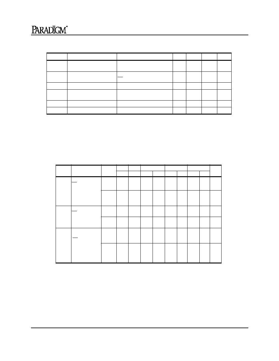
Power Supply Characteristics
NOTE:
All values are maximum guaranteed values.
-9
-10
-12
-15
-20
Symbol Parameter
Com'l Com'l Com'l
Ind.
Com'l
Ind.
Com'l
Ind.
Unit
I
CC
Operating Current
CE = V
IL
SA
175
165
150
160
130
140
120
130
mA
f = f
MAX
= 1/t
RC
V
CC
= Max.
I
OUT
= 0 mA
LA
150
140
130
140
120
130
110
120
mA
I
SB
Standby Current
CE = V
IH
SA
30
30
30
30
30
30
30
30
mA
f = f
MAX
= 1/t
RC
V
CC
= Max.
LA
15
15
15
15
15
15
15
15
mA
I
SB1
Full Standby
Current
CE
V
CC
≠ 0.2V
SA
5
5
5
5
5
5
5
5
mA
f = 0
V
CC
= Max.,
V
IN
V
CC
≠ 0.2V
or
0.2V
LA
2
2
2
5
2
5
2
5
mA
DC Electrical Characteristics
(V
CC
= 3.3V
±
0.3V)
NOTE: 4. V
IL
(min) = ≠3.0V for pulse width less than 20 ns.
Symbol
Parameter
Test Conditions
Min.
Max.
Unit
I
LI
Input Leakage Current
V
CC
= Max., V
IN
= Vss to V
CC
Com'l/
Ind.
≠5
5
µ
A
I
LO
Output Leakage Current
V
CC
= Max.,
CE = V
IH
, V
OUT
= Vss to V
CC
Com'l/
Ind.
≠5
5
µ
A
V
IL
Input Low Voltage
≠0.3
(4)
0.8
V
V
IH
Input High Voltage
2.2
Vcc +
0.3
V
V
OL
Output Low Voltage
I
OL
= 8 mA, V
CC
= Min.
--
0.4
V
V
OH
Output High Voltage
I
OH
= ≠4 mA, V
CC
= Min.
2.4
--
V
PDM31532
Rev. 4.3 - 3/27/98
5
1
2
3
4
5
6
7
8
9
10
11
12
+3.3V
317
351
D
OUT
30 pF
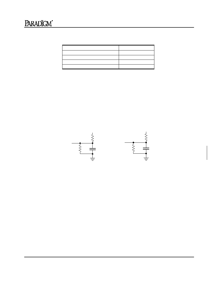
Figure 1. Output Load
Figure 2. Output Load Equivalent
(for t
LZCE
, t
HZCE
, t
LZWE
, t
HZWE,
t
LZOE
, t
HZOE
, t
LZBE
, t
HZBE
)
+3.3V
317
351
D
OUT
5 pF
AC Test Conditions
Input pulse levels
V
SS
to 3.0V
Input rise and fall times
2.5 NS
Input timing reference levels
1.5V
Output reference levels
1.5V
Output load
See Figures 1 and 2

PDM31532
6
Rev. 4.3 - 3/27/98
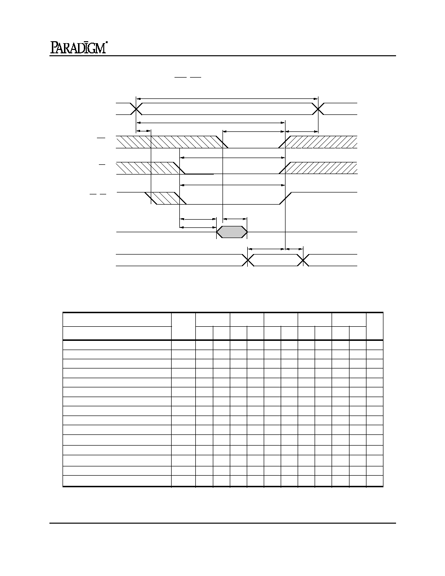
t
AA
t
RC
UB, LB
OE
CE
ADDRESSES
t
OH
t
AOE
t
BA
D
OUT
Output Data Valid
t
LZBE(5)
t
LZOE(5)
t
LZCE(5)
t
ACE
t
HZCE(5)
t
HZOE(5)
t
HZBE(5)
Read Timing Diagram
AC Electrical Characteristics
Description
-9
(7)
≠10
(7)
≠12
≠15
≠20
READ Cycle
Symbol
Min
Max
Min
Max
Min
Max
Min
Max
Min
Max
Unit
READ cycle time
t
RC
9
--
10
--
12
--
15
--
20
--
ns
Address access time
t
AA
--
9
--
10
--
12
--
15
--
20
ns
Chip enable access time
t
ACE
--
9
--
10
--
12
--
15
--
20
ns
Byte access time
t
BA
--
6
--
6
--
7
--
8
--
9
ns
Output hold from address change
t
OH
3
--
3
--
3
--
3
--
3
--
ns
Byte disable to output in low-Z
t
LZBE
0
--
0
--
0
--
0
--
0
--
ns
Byte enable to output in high-Z
t
HZBE
--
7
--
7
--
8
--
9
--
9
ns
Chip enable to output in low-Z
(1, 5)
t
LZCE
3
--
3
--
3
--
3
--
3
--
ns
Chip disable to output high-Z
(1, 5)
t
HZCE
--
6
--
6
--
7
--
8
--
9
ns
Output enable access time
t
AOE
--
6
--
6
--
7
--
8
--
9
ns
Output enable to output in low-Z
(1, 5)
t
LZOE
0
--
0
--
0
--
0
--
0
--
ns
Output disable to output in high-Z
(1, 5)
t
HZOE
--
6
--
6
--
7
--
8
--
9
ns

PDM31532
Rev. 4.3 - 3/27/98
7
1
2
3
4
5
6
7
8
9
10
11
12
Write Cycle 1 Timing Diagram
(8)
(WE Controlled)
t
AW
tAS
t
WC
UB, LB
CE
WE
ADDRESSES
t
WP
t
LZWE(5)
t
CW
t
BW
High Impedance
t
HZWE(5)
t
AH
t
DH
t
DS
Data Stable
(9)
(10)
D
OUT
D
IN
t
AW
tAS
t
WC
UB, LB
CE
WE
ADDRESSES
t
WP
t
CW
High Impedance
t
DH
t
DS
Data Stable
D
OUT
D
IN
t
AH
t
BW
t
LZBE(5)
t
LZCE(5)
t
HZWE(5)
Write Cycle 2 Timing Diagram
(8)
(CE Controlled)
PDM31532
8
Rev. 4.3 - 3/27/98
AC Electrical Characteristics
Description
-9
(7)
-10
(7)
-12
-15
-20
WRITE Cycle
Sym
Min. Max. Min. Max. Min. Max. Min. Max. Min. Max. Unit
WRITE cycle time
t
WC
9
--
10
--
12
--
15
--
20
--
ns
Chip enable to end of write
t
CW
8
--
9
--
10
--
11
--
12
--
ns
Address valid to end of write
t
AW
8
--
9
--
10
--
11
--
12
--
ns
Byte pulse width
t
BW
8
--
9
--
10
--
12
--
13
--
ns
Address setup time
t
AS
0
--
0
--
0
--
0
--
0
--
ns
Address hold from end of write
t
AH
0
--
0
--
0
--
0
--
0
--
ns
Write pulse width
t
WP
7
--
7
--
8
--
9
--
10
--
ns
Data setup time
t
DS
6
--
6
--
7
--
8
--
9
--
ns
Data hold time
t
DH
0
--
0
--
0
--
0
--
0
--
ns
Byte disable to output in low Z
(1, 5, 8)
t
LZBE
1
--
1
--
1
--
1
--
1
--
ns
Byte enable to output in high Z
(1, 5, 8)
t
HZBE
--
7
--
7
--
7
--
8
--
9
ns
Output disable to output in low Z
(1, 5, 8)
t
LZOE
0
--
0
--
0
--
0
--
0
--
ns
Output enable to output in high Z
(1, 5, 8)
t
HZOE
--
7
--
7
--
7
--
8
--
9
ns
Write disable to output in low Z
(1, 5, 8)
t
LZWE
1
--
1
--
1
--
1
--
1
--
ns
Write enable to output in high Z
(1, 5, 8)
t
HZWE
--
7
--
7
--
7
--
8
--
9
ns
Write Cycle 3 Timing Diagram
(8)
(UB, LB Controlled)
t
AW
tAS
t
WC
UB, LB
CE
WE
ADDRESSES
t
WP
t
CW
High Impedance
t
DH
t
DS
Data Stable
D
OUT
D
IN
t
AH
t
BW
t
LZBE(5)
t
LZCE(5)
t
HZWE(5)

PDM31532
Rev. 4.3 - 3/27/98
9
1
2
3
4
5
6
7
8
9
10
11
12
Device Type
Power
Speed
Package
Type
Process
Temp. Range
Preferred
Shipping
Container
Commercial (0
∞
to +70
∞
C)
Industrial (≠40
∞
C to +85
∞
C)
9
Commercial Only
10
Commercial Only
12
15
20
SA
Standard Power
LA
Low Power
Blank
I
A
Automotive ( ≠40
∞
C to +105
∞
C)
Blank Tubes
TR Tape & Reel
TY Tray
PDM31532 - (64Kx16) Static RAM
XXXXX
X
XX
X
X
X
SO
44-pin 400-mil Plastic SOJ
T
44-pin Plastic TSOP (II)
NOTES:
5. Measured with C
L
= 5 pF as in Figure 2. Transition is measured
±
200 mV from steady state voltage
6. At any given temperature and voltage condition, t
HZCE
is less than t
LZCE
and t
HZWE
is less than t
LZWE
.
7. Vcc = 3.3V +5%
8. If OE is HIGH during a write cycle, the outputs are in a high-impedance state during this period.
9. If the CE LOW transition occurs coincident with or after the WE LOW transition, outputs remain in a high
impedance state
10.If the CE HIGH transition occurs coincident with or after the WE HIGH transition, outputs remain in a high
impedance state.
Ordering Information
Faster Memories for a FasterWorld
TM
Notes for AC Tables