Document Outline
- Features
- X
- X
- H
- Hi-Z
- Standby
- L
- H
- L
- DOUT
- Read
- X
- L
- L
- DIN
- Write
- H
- H
- L
- Hi-Z
- Output Disable
- VTERM
- Terminal Voltage with Respect to Vss
- Ö0.5 to +7.0
- Ö0.5 to +7.0
- V
- TBIAS
- Temperature Under Bias
- Ö55 to +125
- Ö65 to +135
- ∞C
- TSTG
- Storage Temperature
- Ö55 to +125
- Ö65 to +150
- ∞C
- PT
- Power Dissipation
- 1.0
- 1.0
- W
- IOUT
- DC Output Current
- 50
- 50
- mA
- Tj
- Maximum Junction Temperature (2)
- 125
- 145
- ∞C
- VCC
- Supply Voltage
- 4.5
- 5.0
- 5.5
- V
- VSS
- Supply Voltage
- 0
- 0
- 0
- V
- Commercial
- Ambient Temperature
- 0
- 25
- 70
- ∞C
- Industrial
- Ambient Temperature
- Ö40
- 25
- 85
- ∞C
- ILI
- Input Leakage Current
- VCC = MAX., VIN = Vss to VCC
- Comêl/
- Ind.
- Ö5
- 5
- Ö1
- 1
- mA
- ILO
- Output Leakage Current
- VCC= MAX.,
- CE = VIH, VOUT = Vss to VCC
- Comêl/
- Ind.
- Ö5
- 5
- Ö1
- 1
- mA
- VIL
- Input Low Voltage
- Ö0.5(1)
- 0.8
- Ö0.5(1)
- 0.8
- V
- VIH
- Input High Voltage
- 2.2
- 6.0
- 2.2
- 6.0
- V
- VOL
- Output Low Voltage
- IOL=8 mA, VCC = Min.
- IOL = 10 mA, VCC = Min.
- Ñ
- Ñ
- 0.4
- 0.5
- Ñ
- Ñ
- 0.4
- 0.5
- V
- VOH
- Output High Voltage
- IOH = Ö4 mA, VCC = Min.
- 2.4
- Ñ
- 2.4
- Ñ
- V
- ICC
- Operating Current
- CE = VIL
- SA
- 210
- 200
- 210
- 190
- 200
- 170
- 180
- 150
- 160
- mA
- f = fMAX = 1/tRC
- VCC = Max
- IOUT = 0 mA
- LA
- 190
- 180
- 190
- 170
- 180
- 150
- 160
- 130
- 140
- mA
- ISB
- Standby Current
- CE = VIH
- SA
- 90
- 80
- 80
- 70
- 70
- 60
- 60
- 50
- 50
- mA
- f = fMAX = 1/tRC
- VCC = Max
- LA
- 90
- 80
- 80
- 70
- 70
- 60
- 60
- 50
- 50
- mA
- ISB1
- Full Standby Current
- CE ≥ VCC Ö 0.2V
- SA
- 20
- 20
- 20
- 20
- 20
- 20
- 20
- 20
- 20
- mA
- f = 0
- VCC = Max
- VIN ≥ VCC Ö 0.2V or £ 0.2V
- LA
- 5
- 5
- 5
- 5
- 5
- 5
- 5
- 5
- 5
- mA
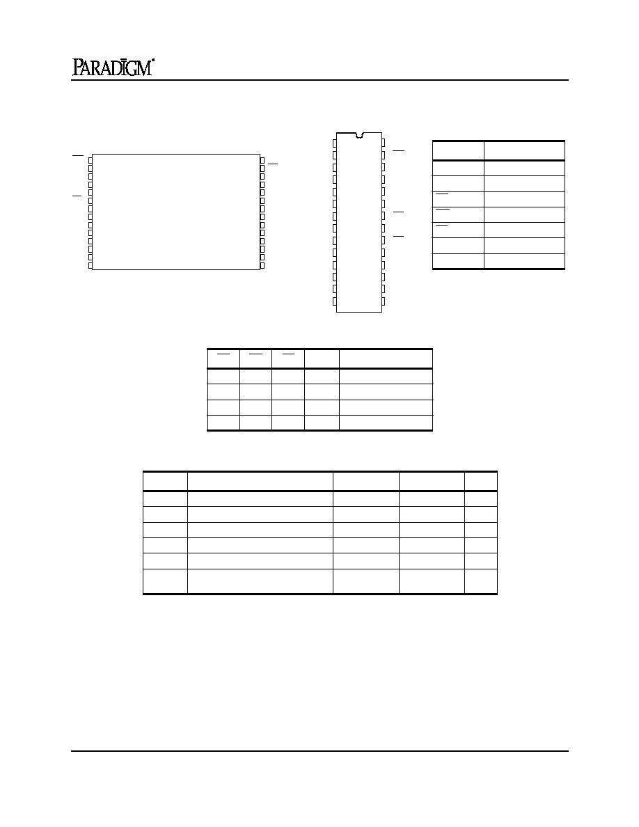
- Pin Configurations
- TSOP (I)
- SOJ
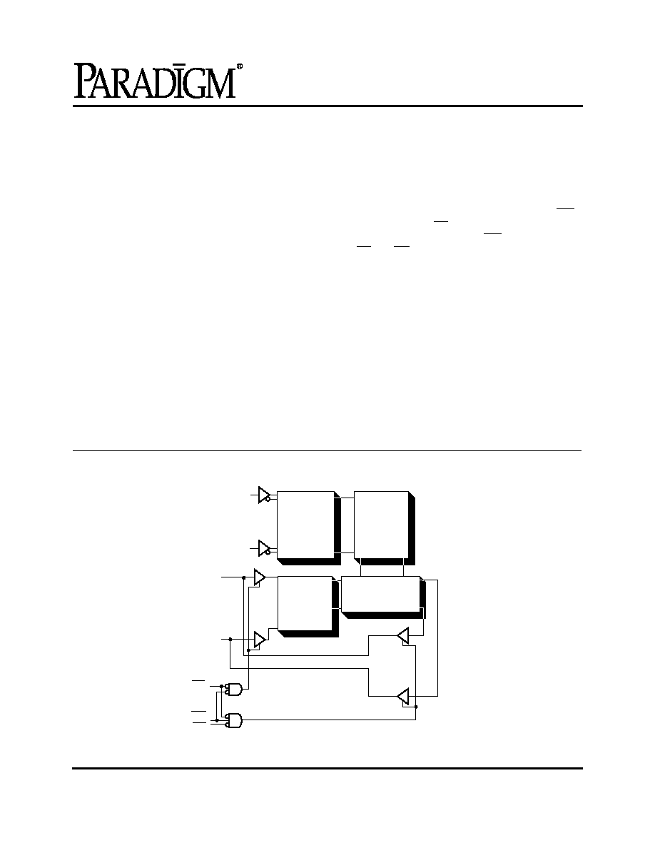
- Functional Block Diagram
- A14-A0
- Address Inputs
- I/O7-I/O0
- Data Inputs/Outputs
- OE
- Output Enable Input
- WE
- Write Enable Input
- CE
- Chip Enable Input
- VCC
- Power (+5V)
- VSS
- Ground
- CIN
- Input Capacitance
- 8
- pF
- COUT
- Output Capacitance
- 8
- pF
- Input pulse levels
- VSS to 3.0V
- Input rise and fall times
- 3 ns
- Input timing reference levels
- 1.5V
- Output reference levels
- 1.5V
- Output load
- See Figures 1 and 2
- READ cycle time
- tRC
- 7
- 8
- 10
- 12
- 15
- ns
- Address access time
- tAA
- 7
- 8
- 10
- 12
- 15
- ns
- Chip enable access time
- tACE
- 7
- 8
- 10
- 12
- 15
- ns
- Output hold from address change
- tOH
- 3
- 3
- 3
- 3
- 3
- ns
- Chip enable to output in low Z(3, 4, 5)
- tLZCE
- 5
- 5
- 5
- 5
- 5
- ns
- Chip disable to output in high Z(3, 4, 5)
- tHZCE
- 5
- 6
- 6
- 6
- 6
- ns
- Chip enable to power up time(4)
- tPU
- 0
- 0
- 0
- 0
- 0
- ns
- Chip disable to power down time(4)
- tPD
- 7
- 8
- 10
- 12
- 15
- ns
- Output enable access time
- tAOE
- 5
- 5
- 5
- 6
- 8
- ns
- Output enable to output in low Z(4, 5)
- tLZOE
- 0
- 0
- 0
- 0
- 0
- ns
- Output disable to output in high Z(4, 5)
- tHZOE
- 5
- 6
- 6
- 6
- 6
- ns
- WRITE cycle time
- tWC
- 7
- 8
- 10
- 12
- 15
- ns
- Chip enable to end of write
- tCW
- 7
- 8
- 10
- 10
- 12
- ns
- Address valid to end of write
- tAW
- 7
- 8
- 10
- 10
- 12
- ns
- Address setup time
- tAS
- 0
- 0
- 0
- 0
- 0
- ns
- Address hold from end of write
- tAH
- 0
- 0
- 0
- 0
- 0
- ns
- Write pulse width
- tWP
- 7
- 8
- 8
- 8
- 11
- ns
- Data setup time
- tDS
- 6
- 7
- 7
- 7
- 7
- ns
- Data hold time
- tDH
- 0
- 0
- 0
- 0
- 0
- ns
- Write disable to output in low Z(4, 5)
- tLZWE
- 0
- 0
- 0
- 0
- 0
- ns
- Write enable to output in high Z(4, 5)
- tHZWE
- 3
- 3
- 3
- 3
- 3
- ns
- VDR
- VCC for Retention Data
- 2
- Ñ
- Ñ
- V
- ICCDR
- Data Retention Current
- CE ≥ VCC Ö 0.2V
- VIN ≥ VCC Ö 0.2V
- or £ 0.2V
- VCC = 2V
- Ñ
- 95
- 500
- mA
- VCC = 3V
- Ñ
- 350
- 750
- mA
- tCDR
- Chip Deselect to Data Retention Time
- 0
- Ñ
- Ñ
- ns
- tR(4)
- Operation Recovery Time
- tRC
- Ñ
- Ñ
- ns
- PDM41256
- 256K Static RAM
- 32K x 8-Bit
Rev. 4.4 - 4/29/98
1
1
2
3
4
5
6
7
8
9
10
11
12
Features
n
High-speed access times
Com'l: 7, 8, 10, 12 and 15ns
Ind'l: 8, 10, 12 and 15ns
(use 15ns for slower designs)
n
Low power operation (typical)
- PDM41256SA
Active: 475 mW
Standby: 100 mW
- PDM41256LA
Active: 425mW
Standby: 25 mW
n
Single +5V (
±
10%) power supply
n
TTL-compatible inputs and outputs
n
Packages
Plastic SOJ (300 mil) - SO
Plastic TSOP (I) - T
Description
The PDM41256 is a high-performance CMOS static
RAM organized as 32,768 x 8 bits. Writing to this
device is accomplished when the write enable (WE)
and the chip enable (CE) inputs are both LOW.
Reading is accomplished when WE remains HIGH
and CE and OE are both LOW.
The PDM41256 operates from a single +5V power
supply and all the inputs and outputs are fully TTL-
compatible. The PDM41256 comes in two versions:
the standard power version PDM41256SA and the
low power version PDM41256LA. Both versions are
functionally the same and differ only in their power
consumption.
The PDM41256 is available in a 28-pin plastic TSOP
(I) and a 28-pin 300-mil plastic SOJ.
A
∑
∑
∑
∑
∑
A
0
14
I/O
∑
∑
I/O
0
7
CE
WE
∑
∑
∑
∑
∑
∑
Addresses
Decoder
Memory
Matrix
Input
Data
Control
Column I/O
∑ ∑ ∑ ∑ ∑
OE
∑
∑
∑
Functional Block Diagram
PDM41256
256K Static RAM
32K x 8-Bit
PDM41256
2
Rev. 4.4 - 4/29/98
OE
A11
A9
A8
A13
WE
Vcc
A14
A12
A7
A6
A5
A4
A3
21
20
19
18
17
16
15
14
13
12
11
10
9
8
A10
CE
I/O7
I/O6
I/O5
I/O4
I/O3
Vss
I/O2
I/O1
I/O0
A0
A1
A2
22
23
24
25
26
27
28
1
2
3
4
5
6
7
1
2
3
4
5
6
7
8
9
10
11
12
15
16
17
18
19
20
21
22
23
24
A14
A12
A7
A6
A5
A4
A3
A2
A1
A0
I/O0
I/O1
I/O2
Vss
Vcc
WE
A13
A8
A9
A11
OE
A10
CE
I/O7
I/O6
I/O5
I/O4
I/O3
13
14
25
26
27
28
Truth Table
NOTE: 1. H = V
IH
, L = V
IL
, X = DON'T CARE
Absolute Maximum Ratings
(1)
NOTE: 1. Stresses greater than those listed under ABSOLUTE MAXIMUM RATINGS may
cause permanent damage to the device. This is a stress rating only and functional
operation of the device at these or any other conditions above those indicated in the
operational sections of this specification is not implied. Exposure to absolute maxi-
mum rating conditions for extended periods may affect reliability.
2. Appropriate thermal calculations should be performed in all cases and specifically for
those where the chosen package has a large thermal resistance (e.g., TSOP). The
calculation should be of the form
: T
j
= T
a
+ P *
ja
where T
a
is the ambient tempera-
ture, P is average operating power and
ja
the thermal resistance of the package. For
this product, use the following
ja
values:
SOJ: 78
o
C/W
TSOP: 112
o
C/W
OE
WE
CE
I/O
MODE
X
X
H
Hi-Z
Standby
L
H
L
D
OUT
Read
X
L
L
D
IN
Write
H
H
L
Hi-Z
Output Disable
Symbol
Rating
Com'l.
Ind.
Unit
V
TERM
Terminal Voltage with Respect to Vss
≠0.5 to +7.0
≠0.5 to +7.0
V
T
BIAS
Temperature Under Bias
≠55 to +125
≠65 to +135
∞
C
T
STG
Storage Temperature
≠55 to +125
≠65 to +150
∞
C
P
T
Power Dissipation
1.0
1.0
W
I
OUT
DC Output Current
50
50
mA
T
j
Maximum Junction Temperature
(2)
125
145
∞
C
Pin Configurations
TSOP (I)
SOJ
Pin Description
Name
Description
A14-A0
Address Inputs
I/O7-I/O0
Data Inputs/Outputs
OE
Output Enable Input
WE
Write Enable Input
CE
Chip Enable Input
V
CC
Power (+5V)
V
SS
Ground
PDM41256
Rev. 4.4 - 4/29/98
3
1
2
3
4
5
6
7
8
9
10
11
12
Recommended DC Operating Conditions
DC Electrical Characteristics
(V
CC
= 5.0V
±
10%)
NOTE:
1. V
IL
(min) = ≠3.0V for pulse width less than 20 ns.
Power Supply Characteristics
SHADED AREA = PRELIMINARY DATA
NOTE:All values are maximum guaranteed values.
Symbol
Parameter
Min.
Typ.
Max.
Unit
V
CC
Supply Voltage
4.5
5.0
5.5
V
V
SS
Supply Voltage
0
0
0
V
Commercial
Ambient Temperature
0
25
70
∞
C
Industrial
Ambient Temperature
≠40
25
85
∞
C
PDM41256SA
PDM41256LA
Unit
Symbol
Parameter
Test Conditions
Min.
Max.
Min.
Max.
I
LI
Input Leakage Current
V
CC
= MAX., V
IN
= Vss to V
CC
Com'l/
Ind.
≠5
5
≠1
1
µ
A
I
LO
Output Leakage Current
V
CC
= MAX.,
CE = V
IH
, V
OUT
= Vss to V
CC
Com'l/
Ind.
≠5
5
≠1
1
µ
A
V
IL
Input Low Voltage
≠0.5
(1)
0.8
≠0.5
(1)
0.8
V
V
IH
Input High Voltage
2.2
6.0
2.2
6.0
V
V
OL
Output Low Voltage
I
OL
=8 mA, V
CC
= Min.
I
OL
= 10 mA, V
CC
= Min.
--
--
0.4
0.5
--
--
0.4
0.5
V
V
OH
Output High Voltage
I
OH
= ≠4 mA, V
CC
= Min.
2.4
--
2.4
--
V
-7
-8
-10
-12
-15
Symbol Parameter
Power Com'l. Com'l. Ind.
Com'l.
Ind.
Com'l. Ind.
Com'l. Ind.
Units
I
CC
Operating Current
CE = V
IL
SA
210
200
210
190
200
170
180
150
160
mA
f = f
MAX
= 1/t
RC
V
CC
= Max
I
OUT
= 0 mA
LA
190
180
190
170
180
150
160
130
140
mA
I
SB
Standby Current
CE = V
IH
SA
90
80
80
70
70
60
60
50
50
mA
f = f
MAX
= 1/t
RC
V
CC
= Max
LA
90
80
80
70
70
60
60
50
50
mA
I
SB1
Full Standby Current
CE
V
CC
≠ 0.2V
SA
20
20
20
20
20
20
20
20
20
mA
f = 0
V
CC
= Max
V
IN
V
CC
≠ 0.2V or
0.2V
LA
5
5
5
5
5
5
5
5
5
mA
PDM41256
4
Rev. 4.4 - 4/29/98
Capacitance
(1)
(T
A
= +25
∞
C, f = 1.0 MHz)
NOTE: 1. This parameter is determined by device characterization but is not production
tested.
AC Test Conditions
Symbol
Parameter
Max.
Unit
C
IN
Input Capacitance
8
pF
C
OUT
Output Capacitance
8
pF
Input pulse levels
V
SS
to 3.0V
Input rise and fall times
3 ns
Input timing reference levels
1.5V
Output reference levels
1.5V
Output load
See Figures 1 and 2
Figure 1. Output Load Equivalent
Figure 2. Output Load Equivalent
(for t
LZCE
, t
HZCE
, t
LZWE
, t
HZWE
, t
LZOE
,
t
HZOE
)
+5V
480
255
D
OUT
30 pF
+5V
480
255
D
OUT
5 pF
5
4
3
2
1
0
0
30
60
90
120
Typical Delta tAA vs Capacitive Loading
Additional Lumped Capacitive Loading (pF)
Delta t
AA
- nS
Figure 3.
PDM41256
Rev. 4.4 - 4/29/98
5
1
2
3
4
5
6
7
8
9
10
11
12
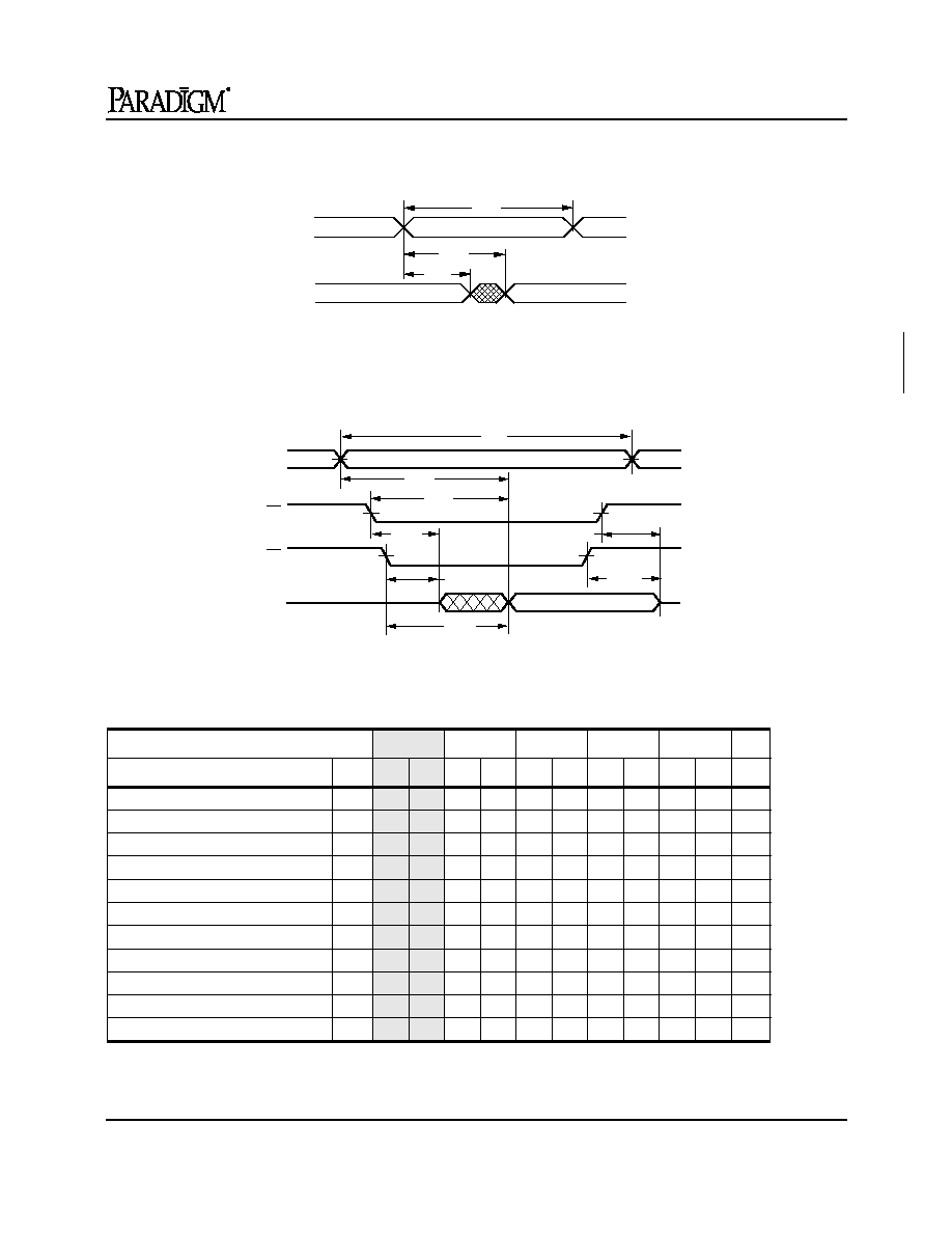
Read Cycle No. 1
(1)
Read Cycle No. 2
(2)
AC Electrical Characteristics
SHADED AREA = PRELIMINARY DATA.
Notes referenced are after Data Retention Table.
Description
--7
(6)
--8
(6)
-10
(6)
-12
-15
READ Cycle
Sym
Min. Max. Min. Max. Min. Max. Min. Max. Min. Max. Units
READ cycle time
t
RC
7
8
10
12
15
ns
Address access time
t
AA
7
8
10
12
15
ns
Chip enable access time
t
ACE
7
8
10
12
15
ns
Output hold from address change
t
OH
3
3
3
3
3
ns
Chip enable to output in low Z
(3, 4, 5)
t
LZCE
5
5
5
5
5
ns
Chip disable to output in high Z
(3, 4, 5)
t
HZCE
5
6
6
6
6
ns
Chip enable to power up time
(4)
t
PU
0
0
0
0
0
ns
Chip disable to power down time
(4)
t
PD
7
8
10
12
15
ns
Output enable access time
t
AOE
5
5
5
6
8
ns
Output enable to output in low Z
(4, 5)
t
LZOE
0
0
0
0
0
ns
Output disable to output in high Z
(4, 5)
t
HZOE
5
6
6
6
6
ns
t RC
tAA
t OH
PREVIOUS DATA VALID
DOUT
ADDR
DATA VALID
t
RC
t
ACE
t
AA
t
LZCE
t
HZCE
t
LZOE
t
HZOE
t
AOE
ADDR
CE
OE
D
OUT
DATA VALID
PDM41256
6
Rev. 4.4 - 4/29/98
Write Cycle No. 1 (Write Enable Controlled)
Write Cycle No. 2 (Chip Enable Controlled)
AC Electrical Characteristics
Description
-7
(6)
-8
(6)
-10
(6)
-12
-15
WRITE Cycle
Sym
Min.
Max.
Min.
Max.
Min.
Max.
Min.
Max.
Min.
Max. Units
WRITE cycle time
t
WC
7
8
10
12
15
ns
Chip enable to end of write
t
CW
7
8
10
10
12
ns
Address valid to end of write
t
AW
7
8
10
10
12
ns
Address setup time
t
AS
0
0
0
0
0
ns
Address hold from end of write
t
AH
0
0
0
0
0
ns
Write pulse width
t
WP
7
8
8
8
11
ns
Data setup time
t
DS
6
7
7
7
7
ns
Data hold time
t
DH
0
0
0
0
0
ns
Write disable to output in low Z
(4, 5)
t
LZWE
0
0
0
0
0
ns
Write enable to output in high Z
(4, 5)
t
HZWE
3
3
3
3
3
ns
t WC
t AW
t CW
t AH
t
AS
t HZWE
HIGH Z
DATA VALID
t LZWE
t DS
t DH
ADDR
CE
t WP
WE
DIN
DOUT
tWC
t AW
tCW
t WP
t DS
DATA VALID
t DH
tAS
ADDR
DIN
UNDEFINED
DON'T CARE
t AH
CE
WE
SHADED AREA = PRELIMINARY DATA
PDM41256
Rev. 4.4 - 4/29/98
7
1
2
3
4
5
6
7
8
9
10
11
12
Low V
CC
Data Retention Waveform
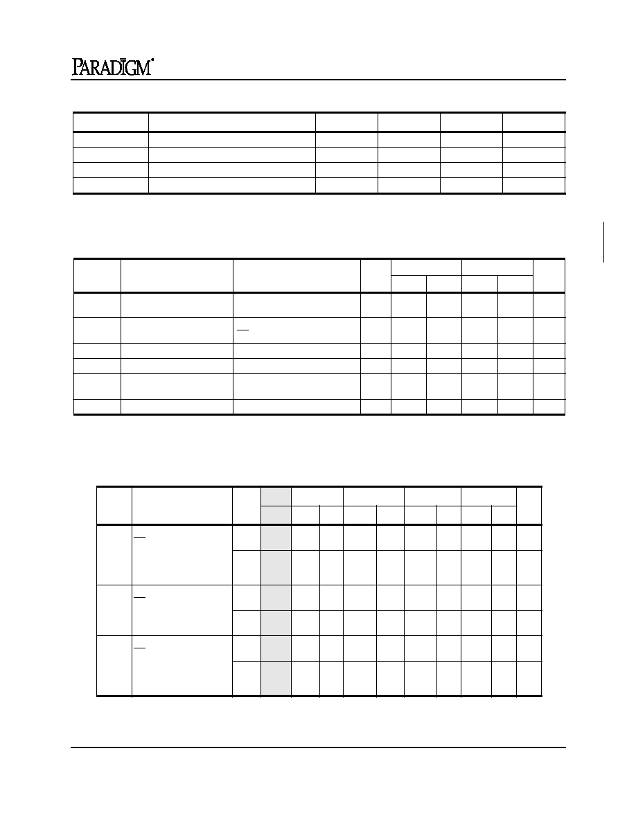
Data Retention Electrical Characteristics (LA Version Only)
NOTES: (For three previous Electrical Characteristics tables)
1. The device is continuously selected. Chip Enable is held in its active state.
2. The address is valid prior to or coincident with the latest occuring Chip Enable.
3. At any given temperature and voltage condition, t
HZCE
is less than t
LZCE
.
4. This parameter is sampled.
5. The parameter is tested with CL = 5 pF as shown in Figure 2. Transition is measured
±
200 mV from steady state voltage
6. Vcc = 5V
±
5%.
Symbol
Parameter
Test Conditions
Min.
Typ.
Max.
Unit
V
DR
V
CC
for Retention Data
2
--
--
V
I
CCDR
Data Retention Current
CE
V
CC
≠ 0.2V
V
IN
V
CC
≠ 0.2V
or
0.2V
V
CC
= 2V
--
95
500
µ
A
V
CC
= 3V
--
350
750
µ
A
t
CDR
Chip Deselect to Data Retention Time
0
--
--
ns
t
R
(4)
Operation Recovery Time
t
RC
--
--
ns
DON'T CARE
VCC
V
V
IH
IL
t
CDR
V
t
R
4.5V
4.5V
Data Retention Mode
CE
DR
VDR
PDM41256
8
Rev. 4.4 - 4/29/98
Ordering Information
Device Type
Power
Speed
Package
Type
Process
Temp. Range
Preferred
Shipping
Container
Commercial (0
∞
to +70
∞
C)
Industrial (≠40
∞
C to +85
∞
C)
7
8
10
12
15
(use 15ns for slower designs)
SA
Standard Power
LA
Low Power
Blank
I
A
Automotive ( ≠40
∞
C to +105
∞
C)
Blank Tubes
TR Tape & Reel
TY Tray
PDM41256- 256K (32Kx8) Static RAM
XXXXX
X
XX
X
X
X
SO
28-pin
300-mil Plastic SOJ
T
28-pin Plastic TSOP (I)
Commercial Only
Faster Memories for a Faster World TM