 | –≠–ª–µ–∫—Ç—Ä–æ–Ω–Ω—ã–π –∫–æ–º–ø–æ–Ω–µ–Ω—Ç: WT5082 | –°–∫–∞—á–∞—Ç—å:  PDF PDF  ZIP ZIP |
Suites 2202-7, 22/F, Tower 6, The Gateway,
9 Canton Road, Tsimshatsui,
Kowloon, Hong Kong
Tel (852) 2123 3289
Fax (852) 2123 3393
E-mail: sales@jesstech.com
HomePage: http://www.jesstech.com
WT5082
1
V0.97
DESCRIPTION
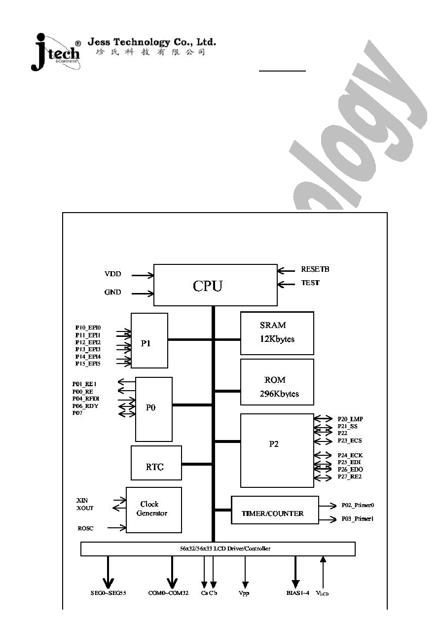
The WT5082 is a high-performance, low-cost, CMOS 8-bit single-chip micro-controller with POCSAG
decoder12KB SRAM 296KB ROM and 56x32 / 56x33 dot-matrix LCD driver embedded, which is
suitable for information paging applications, especially when large number of LCD dots and large ROM
and SRAM space are needed, such as Chinese character display pagers.
This chip has 8-bit CPU, RAM, ROM, I/Os, two timers/counters, interrupt controller, LCD driver and
watchdog timer. To be suitable for portable battery-powered applications, a power saving function is
included.
FEATURES
u
POCSAG pager code decoder
≤
Single crystal support 512, 1200 and 2400 baud rates ( 76.8kHz crystal )
≤
Support 6 RICs addresses and 6 independent frame numbers
≤
Support partial address match facility for address F ( up to 260k addresses are provided )
≤
3 RF control lines ( PLL, quick charge and enable )
≤
Build in data filter ( 16-times over-sampling ) and data bit clock recovery
≤
Interrupt 6502 CPU when there are any status change
≤
DMA or interrupt mode to send the received message data to CPU
u
8-bit single chip Microcontroller with 56x32 / 56x33 LCD driver
u
12Kbytes SRAM ( ~ 2K bits for LCD display SRAM ) , 256 Kbytes character pattern ROM ,
32Kbytes program ROM and 8Kbytes ROM for test program
u
Wide voltage operating range from 2.5 V to 3.6 V
u
Built-in Ring Oscillator with maximum frequency up to 2.0 MHz
u
I/O port (21 pins)
Input port
8 pins
Input/output port
13 pins
u
Watchdog Timer
u
Operating current 0.5mA / 1MHz @ 3V ; providing standby mode and key wake-up mode
≤
Ring OSC OFF and 76.8KHz X'tal OSC ON: current consumption < 60 uA @ 3V

Suites 2202-7, 22/F, Tower 6, The Gateway,
9 Canton Road, Tsimshatsui,
Kowloon, Hong Kong
Tel (852) 2123 3289
Fax (852) 2123 3393
E-mail: sales@jesstech.com
HomePage: http://www.jesstech.com
WT5082
2
V0.97
≤
Both 1Mhz OSC and 76.8KHz X'tal OSC are OFF: current consumption < 5 uA @ 3V
u
Dual timer / counters
u
7-bit EPI ( external port interrupt ) for key wake-up interrupt
u
l-bit EPI ( external port interrupt to 6502 NMI ) for battery remove detect
u
SIO for flex decoder ( 32bit )
u
UART( 10 bits )
u
One PWM signal function
u
2.2V threshold automatic power on reset
u
2.0V low power reset
u
Package: Chip form or 128-pin LQFP ( 14mm x 14mm x 1.4mm )
PACKAGE OUTLINE
Suites 2202-7, 22/F, Tower 6, The Gateway,
9 Canton Road, Tsimshatsui,
Kowloon, Hong Kong
Tel (852) 2123 3289
Fax (852) 2123 3393
E-mail: sales@jesstech.com
HomePage: http://www.jesstech.com
WT5082
3
V0.97
BLOCK DIAGRAM

Suites 2202-7, 22/F, Tower 6, The Gateway,
9 Canton Road, Tsimshatsui,
Kowloon, Hong Kong
Tel (852) 2123 3289
Fax (852) 2123 3393
E-mail: sales@jesstech.com
HomePage: http://www.jesstech.com
WT5082
4
V0.97
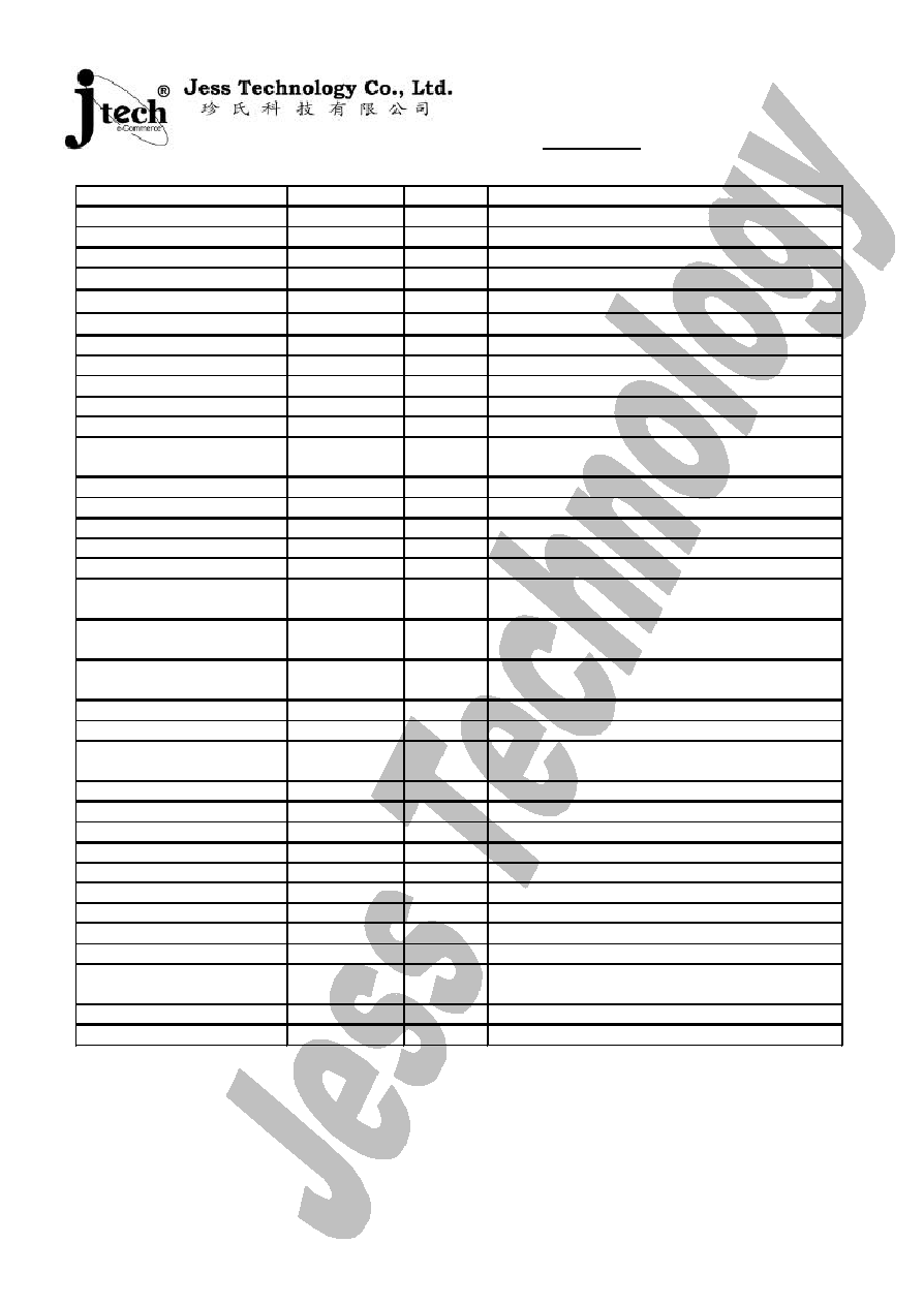
PIN FUNCTION ( 128-pin LQFP )
Suites 2202-7, 22/F, Tower 6, The Gateway,
9 Canton Road, Tsimshatsui,
Kowloon, Hong Kong
Tel (852) 2123 3289
Fax (852) 2123 3393
E-mail: sales@jesstech.com
HomePage: http://www.jesstech.com
WT5082
5
SEG 32 ~ SEG 55
P
Power Source
COM 31 ~ COM 16
50 ~ 73
Output
LCD segment output
COM 32
74 ~ 89
Output
LCD common output
BIAS 1 ~ BIAS 4
Output
LCD common output ( for ICON )
V
LCD
91 ~ 94
Output
LCD bias voltage output
V
PP
Input
LCD voltage supply
Cb
Output
V
RO
*2
Ca
Output
LCD pumping capacitor
P14 _ EPI4
Output
LCD pumping capacitor
P15 _ EPI5
Input
EPI4 , Battery low detect
P20 _ LMP
100
Input
EPI5 , Battery low detect
P21 _ SS
101
I / O
General I/O or Lamp output
P22
102
I / O
General I/O , SS output pin for Serial I/O or UART
serial output
P23 _ ECS
103
I / O
General I/O or PLL _ LE
P24 _ ECK
104
I / O
General I/O for EEPROM CS
P25 _ EDI
105
I / O
General I/O , for EEPROM CK & PLL CK
P26 _ EDO
106
I / O
General I/O for EEPROM DI & PLL DATA
P27 _ RE2
107
I / O
General I/O for EEPROM DO
P06 _ RDY
108
I / O
RF control signal 2 output ( RF enable ) or MISO input
pin for Serial I/O
P01 _ RE1
109
I / O
General I/O or RDY input pin for Serial I/O ; EPI6 or
UART Serial Input
P00 _ RE
110
Output
RF control signal 2 output ( RF enable ) or MISO input
pin for Serial I/O
P04 _ RFDI
111
Output
RF control signal output or SCK output pin for SIO
P07
112
Input
RF signal data input
P10 _ EPI0 ~
113
I / O
General I/O port , Input port for EPI7 or PWM signal
output
P13 _ EPI3
114 - 117
Input
4-bit input port for External interrupt and general input
RESETB
Input
System reset signal input ; low active
GND
P
Ground
XIN
Input
Crystal input
XOUT
Output
Crystal output
VDD
P
Power source
ROSC
Input
Resistor for ring oscillator
P02 _ Ptimer0
I / O
General I/O port or output from ptimer0
P03 _ Ptimer1
I / O
General I/O port or output from ptimer1
768KO
Output
76.8KHz clock output for FLEX decoder or PWM
Enable control signal
TEST
Input
Test pin. High active
COM0
Output
LCD common output
V0.97
APPLICATION DIAGRAM