JIANGSU CHANGJIANG ELECTRONICS TECHNOLOGY CO., LTD
TO-92 Plastic-Encapsulate Transistors
3DD13001
TRANSISTOR
NPN
FEATURES
Power dissipation
P
CM
: 1.25 W
Tamb=25
Collector current
I
CM
: 0.2 A
Collector-base voltage
V
(BR)CBO
: 600 V
Operating and storage junction temperature range
T
J
T
stg
: -55
to +150
ELECTRICAL CHARACTERISTICS
Tamb=25
unless otherwise specified
Parameter
Symbol
Test conditions
MIN
TYP
MAX
UNIT
Collector-base breakdown voltage
V(BR)
CBO
Ic= 100
A
I
E
=0
600
V
Collector-emitter breakdown voltage
V(BR)
CEO
I
C
= 1 mA , I
B
=0
400
V
Emitter-base breakdown voltage
V(BR)
EBO
I
E
= 100
A
I
C
=0
7
V
Collector cut-off current
I
CBO
V
CB
= 600 V , I
E
=0
100
A
Collector cut-off current
I
CEO
V
CE
= 400 V , I
B
=0
200
A
Emitter cut-off current
I
EBO
V
EB
= 7 V , I
C
=0
100
A
h
FE
1
V
CE
= 20 V, I
C
= 20mA
10
70
DC current gain
h
FE
2
V
CE
= 10V, I
C
= 0.25 mA
5
Collector-emitter saturation voltage
V
CE
(sat)
I
C
= 50mA, I
B
= 10 mA
0.5
V
Base-emitter saturation voltage
V
BE
(sat)
I
C
= 50 mA, I
B
= 10mA
1.2
V
Transition frequency
f
T
V
CE
= 20 V, I
C
=20mA
f =
1MHz
8
MHz
Fall time
t
f
0.3
s
Storage time
t
S
I
C
=50mA,
I
B1
=-I
B2
=5mA,
V
CC
=45V
1.5
s
CLASSIFICATION OF h
FE
(1)
Range
10-15
15-20
20-25
25-30
30-35
35-40
40-45
45-50
50-55
55-60
60-65
65-70
1
2
3
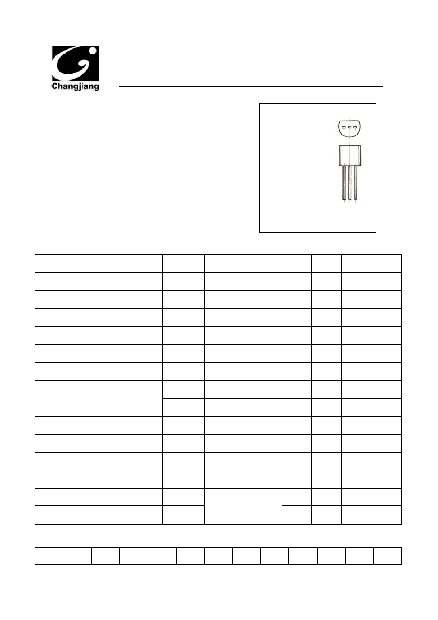
TO
--
92
1.BASE
2.COLLECTOR
3.EMITTER

D
b
E
A
A
1
C
L
D1
e
e1
TO-92 PACKAGE OUTLINE DIMENSIONS
Symbol
A
A1
b
c
D
D1
E
e
e1
L
÷
Min
3.300
1.100
0.380
0.360
4.400
3.430
4.300
2.440
14.100
0.000
Max
3.700
1.400
0.550
0.510
4.700
4.700
2.640
14.500
1.600
0.380
Min
0.130
0.043
0.015
0.014
0.173
0.135
0.169
0.096
0.555
0.000
Max
0.146
0.055
0.022
0.020
0.185
0.185
0.104
0.571
0.063
0.015
Dimensions In Millimeters
Dimensions In Inches
0.050TYP
1.270TYP
