1
Kawasaki LSI
∑
2570 North First Street
∑
Suite 301
∑
San Jose, CA 95131
∑
Tel: (408) 570-0555
∑
Fax: (408) 570-0567
∑
www.klsi.com
Ver. 2.3
KL5KUSB111
USB to HomePNA
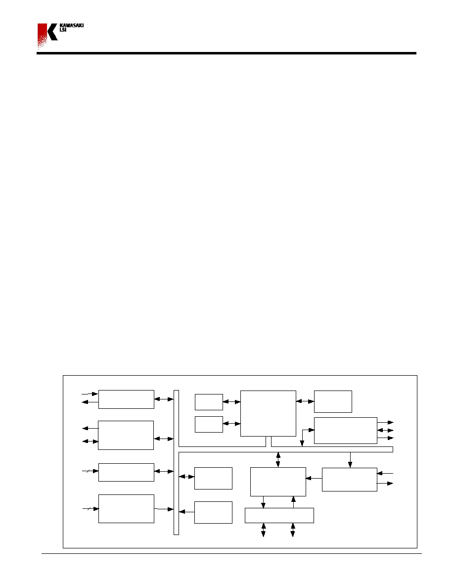
General Description
The Kawasaki KL5KUSB111 Controller is a unique single chip solution developed to interface the Universal Serial
Bus (USB) to HomePNA-Networks and standard 10base-T Networks. The KL5KUSB111 has been specifically
designed to provide a simple solution to communicate with Home Networking Applications at 1 Mb/s and/or 10 Mb/s
Ethernet. By utilizing the Kawasaki's USB to Ethernet technology that has been used throughout the industry. The
USB controller consists of a central 16-bit processor, mask ROM, RAM buffer, clock generator, HomePNA /
Ethernet interface, UART, IRQ, Watchdog Timer, Serial interface, External Memory Interface and Debug UART.
The SIE (Serial Interface Engine) is fully compatible with the USB specification. The Kawasaki USB to HomePNA
controller enables the advantages of Home Networking such as
Shared Internet access, Printer/peripheral
sharing, File and application sharing and Networked gaming.
Features
∑
Advanced 16 Bit processor for USB transaction
processing and control data processing
∑
USB interface ver. 1.0/1.1 compliant
∑
Integrated Transceivers and SIE (Serial Interface
Engine)
∑
Internal Clock Generation
∑
Utilizes low cost external crystal circuitry
∑
1.5K x 16 Internal RAM buffer
∑
Serial Interface for external EEPROM
∑
HomePNA compliant for 1Mb/sec.
∑
Fully IEEE 802.3 compliant 10 Mbit/sec
Ethernet MAC Layer. Interfaces serially of
an external ENDEC PHY.
∑
Debug UART
∑
External memory interface
∑
Compatible with most HomePNA PHY's
∑
Watchdog timer
∑
100 pin LQFP package
Block Diagram
RAM
(3KB)
Timer 0
USB Interface
16 Bit Address / Data Bus
Data -
Data +
Serial
Interface
Engine
Mask ROM
(8KB)
Timer 1
Watchdog
Timer
16 Bit
Processor
UART
Txd
Rxd
1Mb/s PNA
and/or 10Mb/s
Ethernet
8
EEPROM
Serial Interface
DIO
CK
SRAM Interface
A15-0
D15-0
Cntrl.
X2
X1
PLL & Clock
Generator
IRQ
INT 1-0
2

2
Kawasaki LSI
∑
2570 North First Street
∑
Suite 301
∑
San Jose, CA 95131
∑
Tel: (408) 570-0555
∑
Fax: (408) 570-0567
∑
www.klsi.com
Ver. 2.3
KL5KUSB111
USB to HomePNA
KL5KUSB111 Application Block Diagram
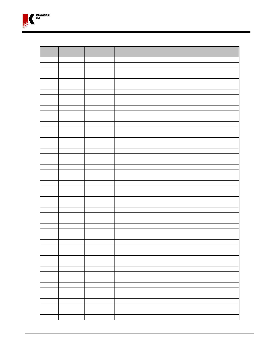
Pin Diagram 100LQFP
Optional
External
Memory
Serial
EEPROM
KL5KUSB111
USB /
Ethernet
PHY
Transformer
USB
Home
Network Phy
or/and
Full duplex
10 Base ≠ T
Ethernet
VDD
GND
VCO_IN
CP_OUT
PLLEN
N/C
N/C
N/C
N/C
N/C
N/C
VDD
GND
PHTXD0
PHCOL
PHTXEN
N/C
N/C
N/C
N/C
N/C
TXD
UGND
VP
VM
UVDD
N/C
N/C
PHTCLK
PHRXCLK
PHCRS
PH_RXD0
X_PCLK
RXD IRQ0 IRQ1 DXA
TSCA
FS
N/C
SERROMD
SERROMCLK
PU#1
PCLK
DRA
OGND
CLK
X2
XA_15
VDD
XA_7
XA_6
XA_5
XA_4
XA_3
XA_2
XA_1
nTST
nRESET
nXROMSEL
nXWR
nXRD
GND
nPDN
N/C
N/C
N/C
N/C
LED_ON
nXRAMSEL
IGND
nXBHE
XA_0
XA_14
OVDD
VDD
XD_15 XD_14
OGND XD_13
XD_12 IGND
XD_11 XD_10
XD_9 XD_8
XD_7 XD_6
XD_5 XD_4
XD_3 XD_2
XD_1 XD_0
XA_13 XA_12
XA_11 XA_10
XA_9 XA_8
1
2
3
4
5
6
7
8
9
10
11
12
13
14
15
16
17
18
19
20
21
22
23
24
25
75
74
73
72
71
70
69
68
67
66
65
64
63
62
61
60
59
58
57
56
55
54
53
52
51
100
99 98
97 96
95 94
93 92
91 90
89 88
87 86
85 84
83 82
81 80
79 78
77 76
26 27
28 29
30 31
32 33
34 35
36 37
38 39
40 41
42 43
44 45
46 47
48 49
50
KL5KUSB111_L

3
Kawasaki LSI
∑
2570 North First Street
∑
Suite 301
∑
San Jose, CA 95131
∑
Tel: (408) 570-0555
∑
Fax: (408) 570-0567
∑
www.klsi.com
Ver. 2.3
KL5KUSB111
USB to HomePNA
Pin Description
Pin #
LQFP
I/O
Pin Name
Description
1
IN
0VDD
VDD
2
IN
GND
GND
3
IN
VCO_IN
PLL VCO IN
4
OUT
CP_OUT
PLL VCO OUT
5
IN
PLLEN
PLL Enable
6
NC
NC
NC
7
NC
NC
NC
8
NC
NC
NC
9
NC
NC
NC
10
NC
NC
NC
11
NC
NC
NC
12
IN
VDD
VDD
13
IN
GND
GND
14
OUT
PHTXD0
Transmit data to PHY
15
IN
PHCOL
Collision input from PHY
16
OUT
PHTXEN
Transmit Enable to PHY
17
NC
NC
NC
18
NC
NC
NC
19
NC
NC
NC
20
NC
NC
NC
21
NC
NC
NC
22
IN/OUT
TXD
UART TXD
23
IN
UGND
USB GND
24
IN/OUT
VP
USB+ Pin
25
IN/OUT
VM
USB- Pin
26
IN
UVDD
USB VDD
27
NC
NC
NC
28
NC
NC
NC
29
IN
PHTXCLK
PHY Transmit Clock
30
IN
PHRXCLK
PHY Receive Clock
31
IN
PHCRS
PHY Carrier Sense
32
IN
PH_RXD0
PHY Serial Receive Data
33
IN/OUT
X_PCLK
External PCLK
34
IN/OUT
RXD
UART RXD
35
IN
IRQ0
IRQ or GPIO10
36
IN
IRQ1
IRQ or GPIO11
37
OUT
DXA
Sport Mode or GPIO7
38
IN
TSCA
Sport Mode or GPIO8
39
IN/OUT
FS
Sport Mode or GPIO9
40
NC
NC
NC
41
IN/OUT
SERROMD
Serial ROM data
42
OUT
SERROMC
LK
Serial ROM clk
43
IN/OUT
PU#1
Pull up to USB + Pin for High Speed
4
Kawasaki LSI
∑
2570 North First Street
∑
Suite 301
∑
San Jose, CA 95131
∑
Tel: (408) 570-0555
∑
Fax: (408) 570-0567
∑
www.klsi.com
Ver. 2.3
KL5KUSB111
USB to HomePNA
Pin #
LQFP
I/O
Pin Name
Description
44
IN
PCLK
Sport Mode or GPIO5
45
IN
DRA
Sport Mode or GPIO6
46
IN
OGND
GND
47
IN
CLK
12MHz Clock/Crystal Input
48
OUT
X2
12MHz Crystal Output
49
OUT
XA_15
External Address Pin
50
IN
VDD
VDD
51
IN
0VDD
VDD
52
OUT
XA_14
External Address Pin
53
OUT
XA_0
External Address Pin
54
OUT
nXBHE
SRAM Byte High Enable
55
IN
IGND
GND
56
OUT
nXRAMSEL
SRAM Byte Low Enable
57
IN/OUT
LED_ON
Turns on 3.3V to TX LED
58
NC
NC
NC
59
NC
NC
NC
60
NC
NC
NC
61
NC
NC
NC
62
IN/OUT
nPDN
Powerdown to PHY(active LO )
63
IN
GND
GND
64
OUT
nXRD
External Memory Read (active LO)
65
OUT
nXWR
External Memory Write (active LO)
66
OUT
nXROMSEL External ROM CS (active LO)
67
IN
nRESET
Reset Pin
68
IN
nTST
Test Pin, NC for Normal Operation
69
OUT
XA_1
External Address Pin
70
OUT
XA_2
External Address Pin
71
OUT
XA_3
External Address Pin
72
OUT
XA_4
External Address Pin
73
OUT
XA_5
External Address Pin
74
OUT
XA_6
External Address Pin
75
OUT
XA_7
External Address Pin
76
OUT
XA_8
External Address Pin
77
OUT
XA_9
External Address Pin
78
OUT
XA_10
External Address Pin
79
OUT
XA_11
External Address Pin
80
OUT
XA_12
External Address Pin
81
OUT
XA_13
External Address Pin
82
IN/OUT
XD_0
External Data Pin
83
IN/OUT
XD_1
External Data Pin
84
IN/OUT
XD_2
External Data Pin
85
IN/OUT
XD_3
External Data Pin
86
IN/OUT
XD_4
External Data Pin
87
IN/OUT
XD_5
External Data Pin
88
IN/OUT
XD_6
External Data Pin
89
IN/OUT
XD_7
External Data Pin
90
IN/OUT
XD_8
External Data Pin
91
IN/OUT
XD_9
External Data Pin
92
IN/OUT
XD_10
External Data Pin

5
Kawasaki LSI
∑
2570 North First Street
∑
Suite 301
∑
San Jose, CA 95131
∑
Tel: (408) 570-0555
∑
Fax: (408) 570-0567
∑
www.klsi.com
Ver. 2.3
KL5KUSB111
USB to HomePNA
Pin #
LQFP
I/O
Pin Name
Description
93
IN/OUT
XD_11
External Data Pin
94
IN
IGND
GND
95
IN/OUT
XD_12
External Data Pin
96
IN/OUT
XD_13
External Data Pin
97
IN
OGND
GND
98
IN/OUT
XD_14
External Data Pin
99
IN/OUT
XD_15
External Data Pin
100
IN
VDD
VDD
Function Description
16 Bit Processor
The integrated 16 bit processor serves as a micro controller for USB peripherals. The processor
can execute approximately five million instructions per second. With this processing power it
allows the design of intelligent peripherals that can process data prior to passing it on to the host
PC, thus improving overall performance of the system. The masked ROM (4K X 16) in the
KL5KUSB111 or external memory contains a specialized instruction set that has been designed
for highly efficient coding of processing algorithms and USB transaction processing.
The 16-bit processor is designed for efficient data execution by having direct access to the RAM
Buffer, external memory, I/O interfaces, and all the control and status registers. The
divide/multiply feature expands the capability of USB peripherals.
The processor supports prioritized vectored hardware interrupts. In addition, as many as 240
software interrupt vectors are available.
The processor provides six addressing modes, supporting memory-to-memory, memory-to-
register, register-to-register, immediate-to-register or immediate-to-memory operations. Register,
direct, immediate, indirect, and indirect indexed addressing modes are supported. In addition,
there is an auto-increment mode in which a register, used as an address pointer is automatically
incremented after each use, making repetitive operations more efficient both from a programming
and a performance standpoint.
The processor features a full set of program control, logical, and integer arithmetic instructions. All
instructions are sixteen bits wide, although some instructions require operands, which may occupy
another one or two words. Several special " short immediate" instructions are available, so that
certain frequently used operations with small constant operand will fit into a 16-bit instruction.
The Processor ≠ Divide/Multiply function
The processor's divide/multiply function contains all the instructions of the base processor that
additionally includes integer divide and multiply instructions. A signed multiply instruction takes
two 16-bit operands and returns a 32-bit result. A signed divide instruction divides a 32-bit
operand by a 16-bit operand.