
128M / 256M X 72 REGISTERED DDR DIMM
Kentron Technologies, Inc.
155 West Street
Wilmington, MA 01887
Phone: 978/988-9100
Fax 978/988-5550
DDR SDRAM FEMMA MODULE
1024 Mega Byte (128M x 72) DDR SDRAM Low Profile
2048 Mega Byte (256M x 72)
Registered 184 Pin DIMM Preliminary
General Description:
This memory module is a high performance 1024 / 2048 Megabyte Registered synchronous
dynamic RAM module organized as 128M /256M x 72 in a 184-pin Dual In-Line Memory Module
(DIMM) package. The module utilizes thirty-six (36) 64M / 128M x4 DDR SDRAM (64ms
Refresh) devices in a TSOP II 400 mil package. A 256 Byte Serial EEPROM contains the
module configuration information. The EEPROM is configured to JEDEC specifications.
These modules offer substantial advances in DRAM operating performance, including the ability
to synchronously burst data at a high rate with automatic column-address generation, interleave
between internal banks in order to hide pre-charge time, and the capability to randomly change
column address on each clock cycle during burst.
Features:
High density:
1024 MB (128M x 72)
2048
MB
(256M
x
72)
Cycle time:
7.5ns (133 MHz)
6.0ns (166 MHz)
Data Rate:
266Mbit/sec/pin (133 MHz)
333Mbit/sec/pin (166 MHz)
JEDEC Standard 184 Pin Registered SDRAM DDR DIMM
PC2100 (DDR266) / PC2700
Single power supply of 2.5V � 10%
Serial Presence Detect
SSTL2 Compatible I/O and Clock
SSTL2 Registered Control & Address Lines
On-board Differential PLL Clock Driver
Auto Precharge and Auto Refresh Modes handled by SDRAM Devices
Programmable Burst Type, Burst Length and CAS Latency of SDRAM devices
Internal Pipeline Operation
Fully Synchronous � all signals registered on positive edge of system clock
Data provided during Reads and Writes at twice the clock frequency
Package Height: 1.20 inches
128M / 256M X 72 REGISTERED DDR DIMM
Kentron Technologies, Inc. (978) 988-9100
Page 2
Rev. (1/03)
Operating Features:
The SDRAM DDR DIMM utilizes a differential clock input for the synchronization. Each
operation of the SDRAM is determined by commands and all operations are referenced to a
positive clock edge. CAS Latency defines the delay from when a Read Command is registered
on a rising clock edge to when the data from the Read Command becomes available at the
outputs. The CAS latency is expressed in terms of clock cycles. This specific DIMM supports 3
and 2 clock cycles.
The burst mode is a very high-speed access mode utilizing an internal column address
generator. Once a column address for the first access is set, following addresses are
automatically generated by the internal column address counter.
All control and address signals are registered on-board and hence delayed by one cycle in
arriving at the SDRAMs. The clock signal is distributed to all SDRAMs via a zero delay PLL
driver. Note that the PLL must be given enough clock cycles to stabilize before any operation
can be given (minimum stabilization time equal to 1 ms).
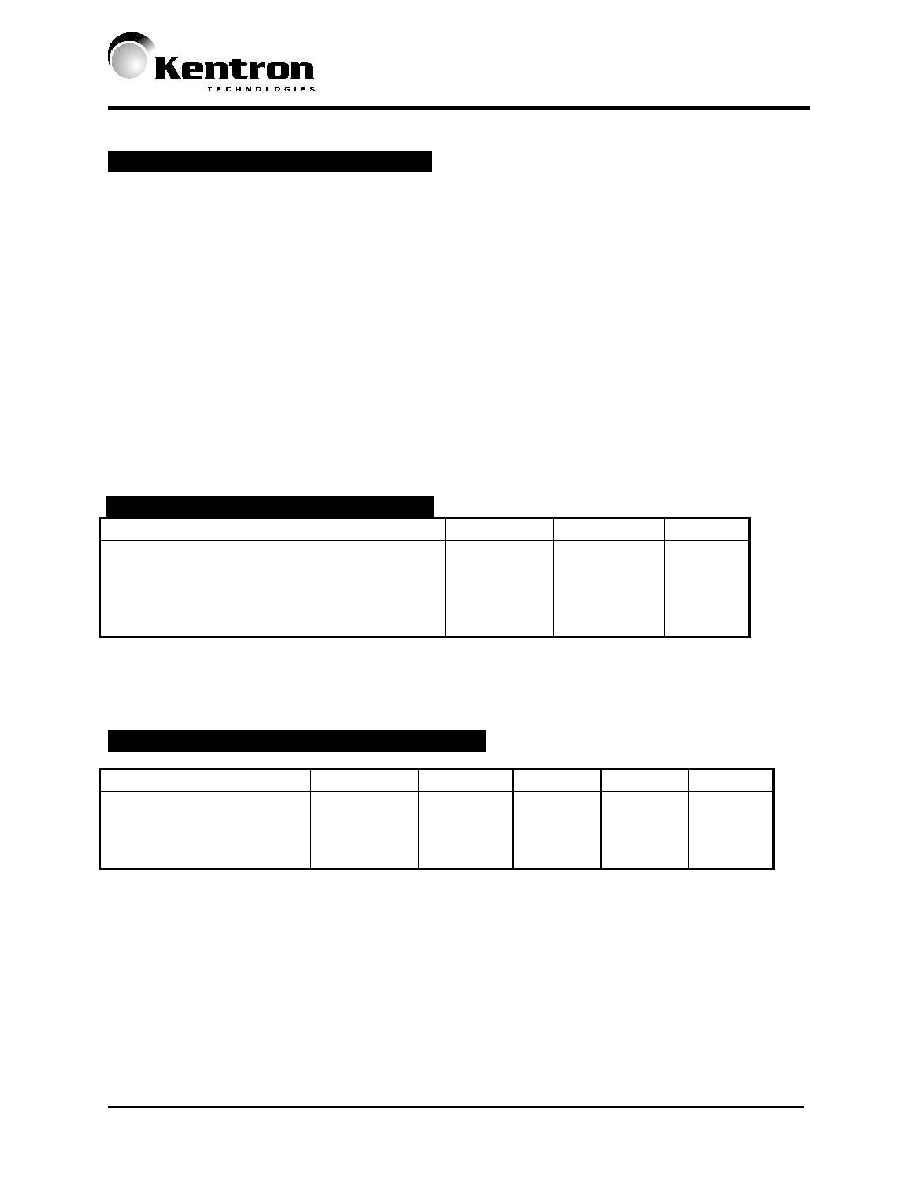
Absolute
Maximum
Ratings*:
Item Symbol
Rating
Unit
Supply voltage (V
CC
Relative to V
SS
) V
dd
-1 ~ 3.6
V
Input/Output Voltage
V
ddq
-1 ~ 3.6
V
Operating temperature
T
opr
70 �C
Storage temperature
T
stg
-55 ~ 150
�C
Short circuit output current
I
out
50
mA
* Permanent device damage may occur if absolute maximum ratings are exceeded. Functional operation
should be restricted to the conditions as detailed in the sections of this data sheet. Exposure to absolute
maximum rating conditions for extended periods may affect device reliability.
Recommended Operating Conditions:
(Voltage referenced to V
dd
. T
A
= 0 to 70 �C)
Item Symbol
Min.
Typ.
Max.
Unit
Supply voltage
V
CC
2.3 2.5
2.7 V
Input high voltage
V
IH
Vref +0.15
-
Vref +0.3
V
Input low voltage
V
IL
-0.3 - 0.8 V
Operating Temperature
T
A
0
+25
70
�C

128M / 256M X 72 REGISTERED DDR DIMM
Kentron Technologies, Inc. (978) 988-9100
Page 3
Rev. (1/03)
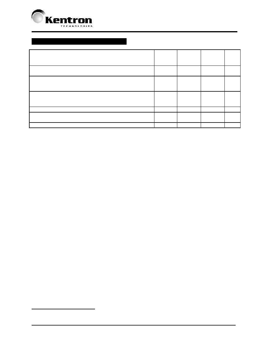
Capacitance:
(TA=25�C, Vdd=2.5V�0.2V)
Parameter Symbol
Max.
Unit
Input capacitance (Address/ WE, CKE0, /CAS, RAS,
/CS0~/CS3)
C
IN
8 pF
Input capacitance (/DQMBs)
C
IN
11 pF
Input capacitance (CK0)
C
IN
4 pF
Input capacitance (DQS0~DQS8)
C
IN
11 pF
Input/Output capacitance (DQ0~DQ63, CB0~CB7)
C
I/O
11 pF
DIMM
Pinout:
No.
Designation No.
Designation No.
Designation No.
Designation No.
Designation
1 VREF
39 DQ26
77 VDDQ
115 A12
153 DQ44
2 DQ0
40 DQ27
78 DQS6
116 VSS
154 RAS/
3 VSS
41 A2
79 DQ50
117 DQ21
155 DQ45
4 DQ1
42 VSS
80 DQ51
118 A11
156 VDDQ
5 DQS0
43 A1
81 VSS
119 DM2/DQS11 157 S0/
6 DQ2
44 CB0
82 VDDID
120 VDD
158 S1/
7 VDD
45 CB1
83 DQ56
121 DQ22
159 DM5/DQS14
8 DQ3
46 VDD
84 DQ57
122 A8
160 VSS
9 NC
47 DQS8
85 VDD
123 DQ23
161 DQ46
10 RESET/
48 A0
86 DQS7
124 VSS
162 DQ47
11 VSS
49 CB2
87 DQ58
125 A6
163 NC,S3/
12 DQ8
50 VSS
88 DQ59
126 DQ28
164 VDDQ
13 DQ9
51 CB3
89 VSS
127 DQ29
165 DQ52
14 DQS1
52 BA1
90 NC
128 VDDQ
166 DQ53
15 VDDQ
53 DQ32
91 SDA
129 DM3/DQS12 167 NC,FETEN
16 DU
(CK1)
54 VDDQ
92 SCL
130 A3
168 VDD
17 DU
(CK1)/
55 DQ33
93 VSS
131 DQ30
169 DM6/DQS15
18 VSS
56 DQS4
94 DQ4
132 VSS
170 DQ54
19
DQ10 57
DQ34 95
DQ5 133
DQ31
171
DQ55
20 DQ11
58 VSS
96 VDDQ
134 CB4
172 VDDQ
21 CCKE0
59 BA0
97 DM0/DQS9
135 CB5
173 NC
22 VDDQ
60 DQ35
98 DQ6
136 VDDQ
174 DQ60
23
DQ16 61
DQ40 99
DQ7 137
CK0 175
DQ61
24 DQ17
62 VDDQ
100 VSS
138 CK0
176 VSS
25 DQS2
63 WE/
101 NC
139 VSS
177 DM7/DQS16
26 VSS
64 DQ41
102 NC
140 DM8/DQS17 178 DQ62
27 A9
65 CAS/
103 A13
141 A10
179 DQ63
28 DQ18
66 VSS
104 VDDQ
142 CB6
180 VDDQ
29 A7
67 DQS5
105 DQ12
143 VDDQ
181 SA0
30
VDDQ 68
DQ42 106
DQ13 144
CB7 182
SA1
31 DQ19
69 DQ43
107 DM1/DQS10 145 VSS
183 SA2
32
A5
70
VDD 108
VDD 146
DQ36
184
VDDSPD
33 DQ24
71 NC,
S2/
109 DQ14
147 DQ37
34
VSS 72
DQ48 110
DQ15 148
VDD
35 DQ25
73 DQ49
111 CKE1
149 DM4/DQS13
36 DQS3
74 VSS
112 VDDQ
150 DQ38
37 A4
75 DU
(CK2)/
113 BA2
151 DQ39
38 VDD
76 DU
(CK2)
114 DQ20
152 VSS
128M / 256M X 72 REGISTERED DDR DIMM
Kentron Technologies, Inc. (978) 988-9100
Page 4
Rev. (1/03)
DC Characteristics:
(V
dd
= 2.5V�.2V, V
SS
=0V, T
A
=0 to + 70�C)
Parameter
1
Symbol
133
MHz
Max.
166
MHz
Max.
Unit
Operating current
(No Burst, T
CK
=min. T
RC
=min.)
I
DD1
4280
4400
mA
Precharge Standby Current
(CKE=V
IL
, T
CK
= min. Bank idle)
(CKE=V
IH
, T
CK
= min. Bank idle)
I
DD2
1850
2210
2070
2430
mA
Active Standby Current
(CKE=V
IL
, T
CK
= min. )
(CKE=V
IH
, T
CK
= min. )
I
DD3
2130
2220
2350
2630
mA
Burst Mode Current (t
CK
=min.) I
DD4
4550 4810
mA
Refresh Current (per DIMM)
(t
CK
=min., t
RC
=min., t
RRD
=min., Auto Refresh)
I
DD5
5540 5820
mA
Self Refresh Current (CKE=V
IL
) I
DD6
1364 1590
mA
1
Module Idd calculated based upon component Idd.

128M / 256M X 72 REGISTERED DDR DIMM
Kentron Technologies, Inc. (978) 988-9100
Page 5
Rev. (1/03)
Block
Diagram: