
Kentron Technologies, Inc.
155 West Street
Wilmington, MA 01887
Phone: (978) 988-9100
Fax (978) 988-5550
www.kentrontech.com
64M x 64 / 72 DDR FEMMA SODIMM
128M x 64 / 72 DDR FEMMA SODIMM
DDR FEMMA SODIMM MODULE
512 MByte (64M x 64 / 72)
1GByte (128M x 64 / 72)
Unbuffered 200 Pin - PC1600/2100 DDR SODIMM
General Description:
This memory module is a high density Unbuffered DDR synchronous dynamic RAM module
organized as x64 or x72 in a 200-pin Small Outline Dual In-Line Memory Module (SODIMM)
package. The module utilizes eighteen (18) X8 DDR SDRAM devices in a TSOP II 400 mil
package. A zero delay buffer drives the input clock to all DDR SDRAM devices. A 256 Byte
Serial EEPROM contains the module configuration information. The EEPROM can be
configured to a customer's specifications.
These modules utilize a double data rate architecture to achieve high speed operation, offering
substantial advances in operating performance, including the ability to synchronously burst
data at a high rate with automatic column-address generation, interleave between internal
banks in order to hide precharge time, and the capability to randomly change column address
on each clock cycle during burst.
Features:
High density: 512 MB (64M x 64) or 512MB (64Mx72 - ECC)
1024 MB (128M x 64) or 1024MB (128Mx72 - ECC)
Cycle time: 10 ns (100 MHz)
7.5 ns (133 MHz)
Double-data-rate architecture; two data transfers per clock cycle
Fast data transfer rates PC1600 or PC2100
JEDEC Standard 200 Pin Unbuffered DDR SODIMM Pinout
Utilizes 200 Mb/s and 266 Mb/s DDR SDRAM components
Single power supply of 2.5V � 0.2V
2.5V I/O (SSTL_2 compatible)
Bi-directional data strobe (DQS) transmitted/received with data
Unbuffered Control and Address Lines
On-board PLL Clock Driver (2 msec settling time)
8K Refresh in 64ms (7.8 usec per row)
Auto Precharge and Auto Refresh Modes handled by SDRAM Devices
Programmable Burst Type, Burst Length and CAS Latency of SDRAM Devices
Serial Presence Detect with EEPROM
Package Height: 1.25 inches (+/- 10mils)
Patented
Kentron Technologies, Inc. (978) 988-9100 Page 2
PRELIMINARY Rev. 01/02
64M x 64 / 72 DDR FEMMA SODIMM
128M x 64 / 72 DDR FEMMA SODIMM
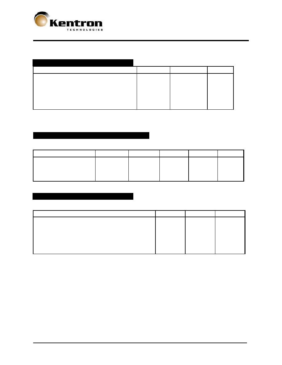
Absolute Maximum Ratings*:
Item
Symbol
Rating
Unit
Supply voltage (V
DD
Relative to V
SS
)
V
DD
-1V to 3.6V
V
Supply voltage
V
DDQ
-1V to 3.6V
V
I/O voltage relative to V
SS
V
I/O
V
DDQ
� 0.5V
Operating temperature
T
opr
0 � 70
�C
Storage temperature
T
stg
-55 �150
�C
Short circuit output current
I
out
50
mA
* Permanent device damage may occur if absolute maximum ratings are exceeded. Functional
operation should be restricted to the conditions as detailed in the sections of this data sheet. Exposure to
absolute maximum rating conditions for extended periods may affect device reliability.
Recommended Operating Conditions:
(Voltage referenced to V
DD
. T
A
= 0 to 70 �C)
Item
Symbol
Min.
Typ.
Max.
Unit
Supply voltage
V
DD
2.3
2.5
2.7
V
I/O Supply Voltage
V
DDQ
2.3
2.7
V
Input high voltage
V
IH
V
REF
+ 0.18
V
dd
+ 0.3
V
Input low voltage
V
IL
-0.3
V
REF
�0.18
V
Capacitance:
(TA=25�C, V
DD
=2.5V�0.2V)
Parameter
Symbol
Max.
Unit
Input capacitance ( /CS0~/CS1)
C
IN
32
pF
Input capacitance (/DQMBs)
C
IN
6.4
pF
Input capacitance (CK0)
C
IN
4
pF
Input capacitance (/RAS, /CAS, /WE, A0-A12)
C
IN
64
pF
Input/Output capacitance
(DQ0~DQ63, CB0~CB7, DQS0~DQS8)
C
I/O
11
pF

Kentron Technologies, Inc. (978) 988-9100 Page 3
PRELIMINARY Rev. 01/02
64M x 64 / 72 DDR FEMMA SODIMM
128M x 64 / 72 DDR FEMMA SODIMM
Pin Names:
A0-A9, A11-A12
Address input
/WE
Write enable
A10/AP
Address input/Auto precharge
DM0-DM8
Data � in mask
BA0-BA1
Bank select
VDD
Power supply
DQ0-DQ63
Data input/output
VSS
Ground
DQS0-DQS8
Data strobe input/output
VREF
Power supply for reference
CB0-CB7
Data check bits
VDDSPD
EEPROM power supply
CK2,/CK2
Clock input
SDA
Serial data I/O
CKE0-CKE1
Clock enable input
SCL
Serial clock
/S0-/S1
Chip select input
SA0-2
Address in EEPROM
/RAS
Row address strobe
VDDID
VDD ID flag
/CAS
Column address strobe
DU
Reserved
Pinout:
No.
Designation
No.
Designation
No.
Designation
No.
Designation
No.
Designation
1
VREF
41
DQ16
81
VDD
121
/S0
161
Vss
2
VREF
42
DQ20
82
VDD
122
/S1
162
VSS
3
VSS
43
DQ17
83
CB3
123
DU
163
DQ48
4
VSS
44
DQ21
84
CB7
124
DU
164
DQ52
5
DQ0
45
VDD
85
DU
125
VSS
165
DQ49
6
DQ4
46
VDD
86
DU
126
VSS
166
DQ53
7
DQ1
47
DQS2
87
VSS
127
DQ32
167
VDD
8
DQ5
48
DM2
88
VSS
128
DQ36
168
VDD
9
VDD
49
DQ18
89
CK2
129
DQ33
169
DQS6
10
VDD
50
DQ22
90
VSS
130
DQ37
170
DM6
11
DQS0
51
VSS
91
/CK2
131
VDD
171
DQ50
12
DM0
52
VSS
92
VDD
132
VDD
172
DQ54
13
DQ2
53
DQ19
93
VDD
133
DQS4
173
Vss
14
DQ6
54
DQ23
94
VDD
134
DM4
174
VSS
15
VSS
55
DQ24
95
CKE1
135
DQ34
175
DQ51
16
VSS
56
DQ28
96
CKE0
136
DQ38
176
DQ55
17
DQ3
57
VDD
97
DU/A13
137
VSS
177
DQ56
18
DQ7
58
VDD
98
DU/BA2
138
VSS
178
DQ60
19
DQ8
59
DQ25
99
A12
139
DQ35
179
VDD
20
DQ12
60
DQ29
100
A11
140
DQ39
180
VDD
21
VDD
61
DQS3
101
A9
141
DQ40
181
DQ57
22
VDD
62
DM3
102
A8
142
DQ44
182
DQ61
23
DQ9
63
VSS
103
VSS
143
VDD
183
DQS7
24
DQ13
64
VSS
104
VSS
144
VDD
184
DM7
25
DQS1
65
DQ26
105
A7
145
DQ41
185
VSS
26
DM1
66
DQ30
106
A6
146
DQ45
186
VSS
27
VSS
67
DQ27
107
A5
147
DQS5
187
DQ58
28
VSS
68
DQ31
108
A4
148
DM5
188
DQ62
29
DQ10
69
VDD
109
A3
149
VSS
189
DQ59
30
DQ14
70
VDD
110
A2
150
VSS
190
DQ63
31
DQ11
71
CB0
111
A1
151
DQ42
191
VDD
32
DQ15
72
CB4
112
A0
152
DQ46
192
VDD
33
VDD
73
CB1
113
VDD
153
DQ43
193
SDA
34
VDD
74
CB5
114
VDD
154
DQ47
194
SA0
35
CK0 (NC)
75
VSS
115
A10/AP
155
VDD
195
SCL
36
VDD
76
VSS
116
BA1
156
VDD
196
SA1
37
/CK0 (NC)
77
DQS8
117
BA0
157
VDD
197
VDDSPD
38
VSS
78
DM8
118
/RAS
158
/CK1 (NC)
198
SA2
39
VSS
79
CB2
119
/WE
159
VSS
199
VDDID
40
VSS
80
CB6
120
/CAS
160
CK1 (NC)
200
DU

Kentron Technologies, Inc. (978) 988-9100 Page 4
PRELIMINARY Rev. 01/02
64M x 64 / 72 DDR FEMMA SODIMM
128M x 64 / 72 DDR FEMMA SODIMM
DC Characteristics:
(V
DD
= 2.5V�.2V, V
SS
=0V, T
A
=0 to + 70�C)
Parameter
1
Symbol
PC2100
Max.
PC1600
Max.
Unit
Operating current
(No Burst, T
CK
=min. T
RC
=min.)
I
DD1
1965
1865
mA
Precharge Standby Current
(CKE=V
IL
, T
CK
= min. Bank idle)
(CKE=V
IH
, T
CK
= min. Bank idle)
I
DD2
200
550
200
550
mA
Active Standby Current
(CKE=V
IL
, T
CK
= min. )
(CKE=V
IH
, T
CK
= min. )
I
DD3
370
820
320
730
mA
Burst Mode Current (t
CK
=min.)
I
DD4
2300
1700
mA
Refresh Current (DIMM both banks)
(t
CK
=min., t
RC
=min., t
RRD
=min., Auto Refresh)
I
DD5
5200
4800
mA
Self Refresh Current (CKE=V
IL
)
I
DD6
208
208
mA
AC Electrical Characteristics:
(V
DD
= 2.5V�.2V, V
SS
=0V, T
A
=0 to + 70�C)
Parameter
Symbol
PC2100
Min.
PC2100
Max.
PC1600
Min.
PC1600
Max.
Unit
Row to row active delay
t
RRD
15
15
ns
RAS to CAS delay
t
RCD
20
20
ns
Row precharge time
t
RP
20
20
ns
Row active time
t
RAS
40
120K
40
120K
ns
Row cycle time
t
RC
65
65
ns
Number of valid output data
3
3
Ea
Clock Cycle Time
t
CK
7.5
10
ns
Clock to Valid Output Delay
T
AC
-0.75
+0.75
-0.8
+0.8
ns
Clock High Pulse Width
t
CH
0.45
0.55
0.45
0.55
ns
Clock Low Pulse Width
t
CL
0.45
0.55
0.45
0.55
ns
Input Setup Time
T
IS
1
1
ns
Input Hold Time
T
IH
0.9
0.9
ns
1
Module Idd calculated based upon Mitsubishi 512Mb component Idd.
Kentron Technologies, Inc. (978) 988-9100 Page 5
PRELIMINARY Rev. 01/02
64M x 64 / 72 DDR FEMMA SODIMM
128M x 64 / 72 DDR FEMMA SODIMM
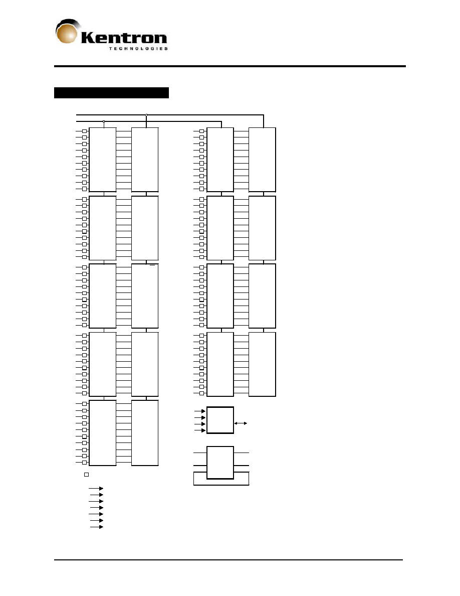
Functional Block Diagram:
/S1
/S0
DQS0
DQS
/CS
DQS
/CS
DQS4
DQS
/CS
DQS
/CS
DM0
DM
DM
DM4
DM
DM
DQ0
IO0
IO0
DQ32
IO0
IO0
DQ1
IO1
D0
IO1
D9
DQ33
IO1
D5
IO1
D14
DQ2
IO2
IO2
DQ34
IO2
IO2
DQ3
IO3
IO3
DQ35
IO3
IO3
DQ4
IO4
IO4
DQ36
IO4
IO4
DQ5
IO5
IO5
DQ37
IO5
IO5
DQ6
IO6
IO6
DQ38
IO6
IO6
DQ7
IO7
IO7
DQ39
IO7
IO7
DQS1
DQS
/CS
DQS
/CS
DQS5
DQS
/CS
DQS
/CS
DM1
DM
DM
DM5
DM
DM
DQ8
IO0
IO0
DQ40
IO0
IO0
DQ9
IO1
D1
IO1
D10
DQ41
IO1
D6
IO1
D15
DQ10
IO2
IO2
DQ42
IO2
IO2
DQ11
IO3
IO3
DQ43
IO3
IO3
DQ12
IO4
IO4
DQ44
IO4
IO4
DQ13
IO5
IO5
DQ45
IO5
IO5
DQ14
IO6
IO6
DQ46
IO6
IO6
DQ15
IO7
IO7
DQ47
IO7
IO7
DQS2
DQS
/CS
DQS
/CS
DQS6
DQS
/CS
DQS
/CS
DM2
DM
DM
DM6
DM
DM
DQ16
IO0
IO0
DQ48
IO0
IO0
DQ17
IO1
D2
IO1
D11
DQ49
IO1
D7
IO1
D16
DQ18
IO2
IO2
DQ50
IO2
IO2
DQ19
IO3
IO3
DQ51
IO3
IO3
DQ20
IO4
IO4
DQ52
IO4
IO4
DQ21
IO5
IO5
DQ53
IO5
IO5
DQ22
IO6
IO6
DQ54
IO6
IO6
DQ23
IO7
IO7
DQ55
IO7
IO7
DQS3
DQS
/CS
DQS
/CS
DQS7
DQS
/CS
DQS
/CS
DM3
DM
DM
DM7
DM
DM
DQ24
IO0
IO0
DQ56
IO0
IO0
DQ25
IO1
D3
IO1
D12
DQ57
IO1
D8
IO1
D17
DQ26
IO2
IO2
DQ58
IO2
IO2
DQ27
IO3
IO3
DQ59
IO3
IO3
DQ28
IO4
IO4
DQ60
IO4
IO4
DQ29
IO5
IO5
DQ61
IO5
IO5
DQ30
IO6
IO6
DQ62
IO6
IO6
DQ31
IO7
IO7
DQ63
IO7
IO7
DQS8
DQS
/CS
DQS
/CS
DM8
DM
DM
SCL
CB0
IO0
IO0
SA0
A0
CB1
IO1
D4
IO1
D13
SA1
A1
SDA
CB2
IO2
IO2
SA2
A2
CB3
IO3
IO3
CB4
IO4
IO4
CB5
IO5
IO5
CK0
CLK
D0-D17
CB6
IO6
IO6
CB7
IO7
IO7
/CK0
/CLK
D0-D17
All resistor values are 22 ohms.
BA0-BA1
SDRAMS D0-D17
A0-AN
SDRAMS D0-D17
/RAS
SDRAMS D0-D17
/CAS
SDRAMS D0-D17
/WE
SDRAMS D0-D17
CKE0
SDRAMS D0-D17
CKE1
SDRAMS D0-D17
PLL
R
R
R
R
R
R
R
R
R
R
R
R
R
R
R
R
R
R
R
R
R
R
R
R
R
R
R
R
R
R
R
R
R
R
R
R
R
R
R
R
R
R
R
R
R
R
R
R
R
R
R
R
R
R
R
R
R
R
R
R
R
R
R
R
R
R
R
R
R
R
R
R
R
R
R
R
R
R
R
R
R
R
R
R
R
R
R
R
R
R
R
R
R
R
R
R
R
R
R
R