
King Billion Electronics Co., Ltd
HE83R123
HE80000 Series
April 28, 2003
1
V1.0E
This specification is subject to change without notice. Please contact sales person for the latest version before use.
- Table of Contents -
1.
General Description ___________________________________________________________________1
2.
Features _____________________________________________________________________________2
3.
Pin Description _______________________________________________________________________3
4.
LCD Power Supply____________________________________________________________________5
5.
LCDC Control register_________________________________________________________________5
6.
LCD RAM map_______________________________________________________________________5
7.
Oscillators ___________________________________________________________________________5
8.
General Purpose I/O___________________________________________________________________5
9.
Timer1 ______________________________________________________________________________5
10.
Timer2 ____________________________________________________________________________5
11.
Watch Dog Timer ___________________________________________________________________5
12.
Pulse-Width Modulation _____________________________________________________________5
13.
Summary of Registers and Mask Options _______________________________________________5
14.
Absolute Maximum Rating ___________________________________________________________5
15.
Recommended Operating Conditions __________________________________________________5
16.
AC/DC Characteristics ______________________________________________________________5
17.
Application Circuit__________________________________________________________________5
1. General Description
HE83R123 is a member of 8-bit MCU series developed by King Billion. 32 LCD segment driver pins are
multiplexed with I/O pins to provide flexibility of wide variety of combinations to suit the needs of
applications Users can choose any one of combinations from 320 dots LCD Driver with 8 Bit I/O Port to
64 dots LCD Driver with 40-bit I/O Port, etc. by mask option. The built-in LCD power regulator can
provide stable LCD display effect over wide range of battery voltage. The Pulse Width Modulation with
complementary outputs provides the complete speech output mechanism. The 64K ROM can store around
20 second of speech. This chip is applicable to the small/medium systems such as LCD Games, Perpetual
Calendar etc. The instruction set or HE80000 easy to learn and use. Most of instructions take only 3
oscillator clocks. This chip is suitable for the applications that require higher performance.

King Billion Electronics Co., Ltd
HE83R123
HE80000 Series
April 28, 2003
2
V1.0E
This specification is subject to change without notice. Please contact sales person for the latest version before use.
2. Features
Operation Voltage:
2.4V ~ 5.5V
System Clock:
DC ~ 8 MHz @ 5.0V
DC ~ 4 MHz @ 2.4V
Internal
ROM:
64
KB
Internal
RAM:
256
Bytes
Dual Clock System:
Fast clock:
32768 ~ 8M Hz
Slow clock: 32768 Hz
4 Operation Modes:
Fast, Slow, Idle, Sleep modes.
Watch Dog Timer to prevent deadlock condition.
40-bit Bi-directional I/O port with push-pull or Open-Drain output type selectable for each I/O
pin by mask option. 32 of them are multiplexed with LCD segment pins.
64 (8 COM x 8 SEG) ~ 320 (8 COM x 40 SEG) dot LCD driver.
Built-in LCD power regulator to provide stable working voltage (~3Volt)
When VDD2.4Volt, LV4 output voltage around 3volts.
When VDD2.4VoltLV4, 3, 2, 1 output voltage will going down with VDD
Complementary Pulse-Width Modulation outputs.
Two external interrupts and two internal timer interrupts.
Two 16-bit timers.
Instruction set: 32 instructions with 4 addressing modes.
Application field: LCD Games, Perpetual Calendar, etc.

King Billion Electronics Co., Ltd
HE83R123
HE80000 Series
April 28, 2003
3
V1.0E
This specification is subject to change without notice. Please contact sales person for the latest version before use.
3. Pin Description
HE83R123
1
2
3
4
5
6
7
8
9
10
11
12
13
14
15
16
17
18 19 20 21 22 23 24 25 26 27 28 29 30 31 32 33 34 35 36
37
38
39
40
41
42
43
44
45
46
47
48
49
50
51
52
53
54
55
56
57
58
59
60
61
62
63
64
65
66
67
68
69
70
71
72
73
74
75
VDD
PWMP
PWMN
GND
PRT177
PRT176
PRT175
PRT174
PRT173
PRT172
PRT171
PRT170
PRT157
PRT156
PRT155
PRT154
PRT153
PR
T
1
52
PR
T
1
51
PR
T
1
50
PR
T
1
47
PR
T
1
46
PR
T
1
45
PR
T
1
44
PR
T
1
43
PR
T
1
42
PR
T
1
41
PR
T
1
40
PR
T
1
17
PR
T
1
16
PR
T
1
15
PR
T
1
14
PR
T
1
13
PR
T
1
12
PR
T
1
11
PR
T
1
10
SEG7
SEG6
SEG5
SEG4
SEG3
SEG2
SEG1
SEG0
COM7
COM6
COM5
COM4
COM3
COM2
COM1
COM0
LC1
LC2
LVF
LV1
LV2
LV3
LV4
GN
D
RS
T
P
FX
O
FX
I
TS
TP
SXO
SXI
VD
D
PR
T
D
7
PR
T
D
6
PR
T
D
5
PR
T
D
4
PR
T
D
3
PR
T
D
2
PR
T
D
1
PR
T
D
0
Pin Name
Pin # I/O
Description
VDD
1
P Dedicated Power for Pulse Width Modulation output.
PWMP 2
O
Pulse
Width
Modulation
output.
PWMN
3
O Complementary output to PWMP.
GND
4
P Dedicated Power for Pulse Width Modulation output.
PRT17[7..0] 5 ~ 12
B/
O
8-bit bi-directional I/O port 17 is shared with LCD segment pads SEG[39..32].
The function of the pad can be selected individually by mask options
MO_LIO17[7..0]. (`1' for LCD and `0' for I/O).
The output type of I/O pad can also be selected by mask option MO_17PP[7..0]
(1 for push-pull and `0' for open-drain).
As the output structure of I/O pad does not contain tri-state buffer. When using
the I/O as input, "1" must be outputted before reading.
PRT15[7..0] 13 ~ 20
B/
O
8-bit bi-directional I/O port 15 is shared with LCD segment pads SEG[31..24].
The function of the pad can be selected individually by mask options
MO_LIO15[7..0]. (`1' for LCD and `0' for I/O).
The output type of I/O pad can also be selected by mask option MO_15PP[7..0]
(1 for push-pull and `0' for open-drain).
As the output structure of I/O pad does not contain tri-state buffer. When using
the I/O as input, "1" must be outputted before reading.
PRT14[7..0] 21 ~ 28
B/
O
8-bit bi-directional I/O port 14 is shared with LCD segment pads SEG[23..16].
The function of the pad can be selected individually by mask options
MO_LIO14[7..0]. (`1' for LCD and `0' for I/O).
The output type of I/O pad can also be selected by mask option MO_14PP[7..0]
(1 for push-pull and `0' for open-drain).
As the output structure of I/O pad does not contain tri-state buffer. When using
King Billion Electronics Co., Ltd
HE83R123
HE80000 Series
April 28, 2003
4
V1.0E
This specification is subject to change without notice. Please contact sales person for the latest version before use.
Pin Name
Pin # I/O
Description
the I/O as input, "1" must be outputted before reading.
PRT11[7..0] 29 ~ 36
B/
O
8-bit bi-directional I/O port 11 is shared with LCD segment pads SEG[15..8]. The
function of the pad can be selected individually by mask options
MO_LIO11[7..0]. (`1' for LCD and `0' for I/O).
The output type of I/O pad can also be selected by mask option MO_11PP[7..0]
(1 for push-pull and `0' for open-drain).
As the output structure of I/O pad does not contain tri-state buffer. When using
the I/O as input, "1" must be outputted before reading.
SEG[7..0]
37 ~ 44
O LCD SEGMENT SEG[7..0] outputs.
COM[7..0] 45 ~ 52
O LCD COMMON Driver pads.
LC1 53 B
Charge Pump Capacitor Pin
LC2 54 B
Charge Pump Capacitor Pin
LVF
55
I
Regulator Feedback input.
The regulator output voltage can be adjusted by
the resistor between LV1 and LVF pads
LV1
56
B LCD Charge Pump Voltage V1
LV2
57
B LCD Charge Pump Voltage V2
LV3
58
B LCD Charge Pump Voltage V3
LV4
59
B LCD Charge Pump Voltage V4
GND
60
P Power ground Input.
RSTP_N 61
I
System Reset input pin. Level trigger, active low on this pin will put the chip in
reset state.
FXO,
FXI
62, 63
O,
B
External fast clock pin. Two types of oscillator can be selected by MO_FXTAL
(`0' for RC type and `1' for crystal type). For RC type oscillator, one resistor need
to be connected between FXI and GND. For crystal oscillator, one crystal need to
be placed between FXI and FXO. Please refer to application for details.
TSTP_P 64
I
Test input pin. Please bond this pad and reserve a test point on PCB for
debugging. But for improving ESD, please connect this point with zero Ohm
resistor to GND
.
SXO,
SXI
65, 66
O,
I
External slow clock pins. Slow clock is clock source for LCD display, TIMER1,
Time-Base and other internal blocks. Both crystal and RC oscillator are provided.
The slow clock type can be selected by mask option MO_SXTAL. Choose `0' for
RC type and `1' for crystal oscillator.
VDD 67 P
Positive power Input. 0.1 �F decoupling capacitors should be placed as close to
IC VDD and GND pads as possible for best decoupling effect.
PRTD[7..0] 68 ~ 75
B
8-bit bi-directional general purpose I/O port D. The output type of I/O pad can
also be selected by mask option MO_DPP[7..0] (`1' for push-pull and `0' for
open-drain).
As the output structure of I/O pad does not contain tri-state buffer. When using
the I/O as input, `1' must be outputted before reading the pin.
PRTD[7..2] can be used as wake-up pins. PRTD[7..6] can be used as external
interrupt sources.
King Billion Electronics Co., Ltd
HE83R123
HE80000 Series
April 28, 2003
5
V1.0E
This specification is subject to change without notice. Please contact sales person for the latest version before use.
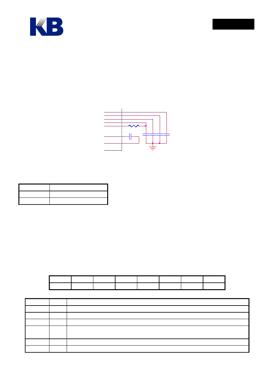
4. LCD Power Supply
The LCD power supply is equipped with input power regulator, voltage charge pumt, and bias voltage
generating resistor network. The input power of MCU is regulated and multiplied by 4 times to generate
LCD bias for LCD driver. The regulator output voltage can be adjusted by the resistor between LV1 and
LVF pads.
LV4
LV3
LV2
LV1
LVF
LC2
LC1
104
0.1uF
R
0.1uF
0.1uF
0.1uF
With the regulated LCD power, the LCD display can give steady visual effect over a wide range of
operating voltage. The built-in regulator must be enabled by mask option MO_ LVRG to function.
MO_LVRG Function
0
Disable LCD regulator
1
Enable LCD regulator
Please note that to emulate the visual effect of 1/4 bias on the ICE 3.X version the LR2 and LR3 on the
top board need be shorted.
5. LCDC Control register
LCD Control Register LCDC controls the functions of LCD driver; such as contrast level, LCD
waveform type, On/Off, Blank, etc.
LCDC
bit 7
bit 6
bit 5
bit 4
bit 3
bit 2
bit 1
bit 0
- - - - -
TYPE BLANK
LCDE
Field Value
Function
TYPE 0
Select
Type
A
LCD
waveform
1
Select
Type
B
LCD
waveform
BLANK 0 Normal
display
1
LCD display blanked. LCD driver changes only COM output signal, SEG
signal remains unchanged.
LCDE
0
LCD driver disabled, LCD driver has no output signal.
1
LCD driver Enabled