 | –≠–ª–µ–∫—Ç—Ä–æ–Ω–Ω—ã–π –∫–æ–º–ø–æ–Ω–µ–Ω—Ç: HF88S05 | –°–∫–∞—á–∞—Ç—å:  PDF PDF  ZIP ZIP |

Command Mode SRAM HF88S05
-1- 02/07/01
Preliminary Product Specification
Product Name
Command Mode SRAM
KB Doc. No.
HF88S05.doc
KB Product. No.
HF88S05
≠ Table of Contents ≠
1. General Description _____________________________________________________2
2. Features ______________________________________________________________2
3. Pin Description_________________________________________________________3
4. Pad Diagram __________________________________________________________4
5. Pad Coordinates ________________________________________________________4
6. Function Block Diagram _________________________________________________5
7. Parallel Mode __________________________________________________________6
7.1.
Parallel Write Command Mode __________________________________________6
7.2.
Parallel Write Data Mode ______________________________________________7
7.3.
Parallel Read Data Mode_______________________________________________7
7.4.
Parallel Read Checksum Mode __________________________________________7
8. Serial Mode ___________________________________________________________8
8.1.
Bi-directional Synchronous Serial Data Interface ___________________________8
8.2.
Serial Write Command Mode____________________________________________9
8.3.
Serial Write Data Mode ________________________________________________9
8.4.
Serial Read Data Mode _______________________________________________10
8.5.
Serial Read Checksum Mode___________________________________________10
9. Power consideration____________________________________________________ 11
10.
Absolute Maximum Rating ____________________________________________ 11
11.
AC Electrical Characteristics __________________________________________ 11
12.
Electrical Characteristics______________________________________________12
13.
Application Circuit___________________________________________________12

Command Mode SRAM HF88S05
-2- 02/07/01
1. General Description
The HF88S05 is a command mode SRAM device. It features dual (parallel and serial)
command access modes. Multiple device array can be accessed with only minimal
additional device select pin. Simple Exclusive Or checksum provides error detection during
data transfer between MCU and the device. The interface logic and protocol include setting
up the starting address for data transfer, writing data into RAM, as well as read it back for
verification, and error checking by Exclusive OR checksum. It can be used for Read/Write
memory extension for all KB's MCUs.
Chip Select pins allows array of HF88S05 devices are used simultaneously for both parallel
and serial transfer mode. In the serial mode, the HF88S05 is connected in daisy chain
configuration to minimize the I/O pins required to use multi-chip array, while in parallel
mode, the devices share most of the control pins and data bus except the chip select pins.
2. Features
Dual (parallel and serial) command access modes.
Address automatically increment with each Read/Write data access.
Exclusive or checksum error detection
Multiple chip array is allowed with easy addressing logic
Read access voltage range 2.7V ~ 5.5V
Organization
- Memory Cell Array: 64K x 8
Package ≠ Dice form

Command Mode SRAM HF88S05
-3- 02/07/01
3. Pin Description
HF88S05
13
11
10
18
5
15
16
12
9
8
7
6
1
4
14
17
3
2
D7
D5
D4
VDD
R_WN
SDI
SDO
D6
D3
D2
D1
D0
P_SN
D_CN
SCLK
CS1
CS0N
VSS
Symbol Pin
No.
I/O Description
P_Sn
I Input to select either parallel (when `1') or serial (when `0') interface is
used for transferring data.
VSS
I
Negative power supply of the device
CS0n
I CS0n is active low chip select input pin. The device is selected when
CS1 is high and CS0n is low simultaneously. Otherwise, it is deselected.
D_Cn
I Input to select either the SRAM or Registers (TPP, TPH, TPL, Mode or
Checksum) operations.
R_Wn
I Input to select either a Read operation (when `1') or a write operation
(when `0') is to be performed.
D0 ~ D7
I/O Bi-directional data bus for parallel transfer mode.
SCLK/
Strobe
I This pin is shared between parallel and serial modes. In serial mode,
this pin is Serial Clock SCLK for transferring the data from/to SDI/SDO.
In parallel mode, it is the strobe signal used to write the registers and
SRAM as well as read the checksum and contents of SRAM. This pin is
equipped with Schmidt type input structure to prevent the input from
chattering due to slow rising clock source transition.
SDI
I
Serial Data Input for writing to either Registers or SRAM.
SDO
O Serial Data Output for reading data from either Checksum Register or
SRAM.
CS1
I
CS1 is active high chip select input. The device is selected when CS1 is
high and CS0n is low simultaneously. Otherwise, it is deselected.
VDD
I
Positive power supply of the device

Command Mode SRAM HF88S05
-4- 02/07/01
4. Pad Diagram
5. Pad Coordinates
Pin
number
Pin
name
X
coordinate
Y
coordinate
Pin
number
Pin
name
X
coordinate Y coordinate
1
P_SN
-1970.5
1260.4
12
D4
1150.32
-1088.97
2
VSS
-1970.5
960.41
13
D5
1375.93
-1088.97
3
VSS
-1970.5
707.54
14
D6
1762.16
-1088.97
4
VSS
-1970.5
394.22
15
D7
1964.53
-759.28
5
CS0N
-1970.5
159.23
16
SCLK
1964.53
-538.44
6
D_CN
-1970.5
-177.15
17
SDI
1964.53
-221.71
7
R_WN
-1970.5
-465.52
18
SDO
1964.53
-0.91
8
D0
-1970.5
-780.53
19
CS1
1964.53
347.7
9
D1
-1725.02
-1088.97
20
VDD
1964.53
600.92
10
D2
-1521.22
-1088.97
21
VDD
1964.53
831.74
11
D3
-1152.68
-1088.97
22
VDD
1964.53
1114.36

Command Mode SRAM HF88S05
-5- 02/07/01
6. Function Block Diagram
Several registers are used in the interface logic. The functions of the registers are described
below and their initial values are as indicated in the following table.
SDO
TPP
TPL
TP[15..0]
TPH
S
CLK/S
tro
b
e
SDI
XOR
CS1
D[
7..0]
Static
D_Cn
DIN[7..0]
S2P
P_Sn
MUX
+ 1
DOUT[7..0]
CS0n
CHKSUM
RAM
MUX
R_Wn
ARRAY
64Kx8
MUX
The Table Pointer register keeps the address of SRAM being written to or read from. It will
automatically increment by one with each read/write access, but remains unchanged when
writing command or reading checksum.
Register Type
Description
Initial
Value
TPL
W Address register 0 for A7 ~ A0
"--------"
TPH
W Address register 1 for A15 ~ A8
"--------"
TPP
W Address register 2 for A23 ~ A16
"--------"
Checksum
R XOR checksum of data
"--------"

Command Mode SRAM HF88S05
-6- 02/07/01
The Checksum Register keeps the Exclusive OR checksum of the data bytes as they are
written to/read from SRAM. The Checksum register cannot be written but it is cleared by
any access to the TPL, TPH and TPP registers.
7. Parallel Mode
When in parallel mode, an 8-bit data bus D[7..0] are used to transfer information between
MCU and SRAM. The advantage of parallel transfer mode is that higher speed can be
achieved. To operate in parallel mode, the P_Sn pin should be driven with high level
voltage.
7.1. Parallel Write Command Mode
Loading of Addresses and Mode Register in parallel mode are by asserting the Strobe (going
low and then high) in write command mode (both R_Wn and D_Cn are low), which will also
clear the CHKSUM register at the same time. After the previous data transfer or when the
device is just selected (CS1 is high and CS0n is low), the command data will be written to
registers in the order of TPL, TPH, TPP, then Mode, TPL... So when unsure, a dummy data
read or deselect and select the device again will reset the register select.
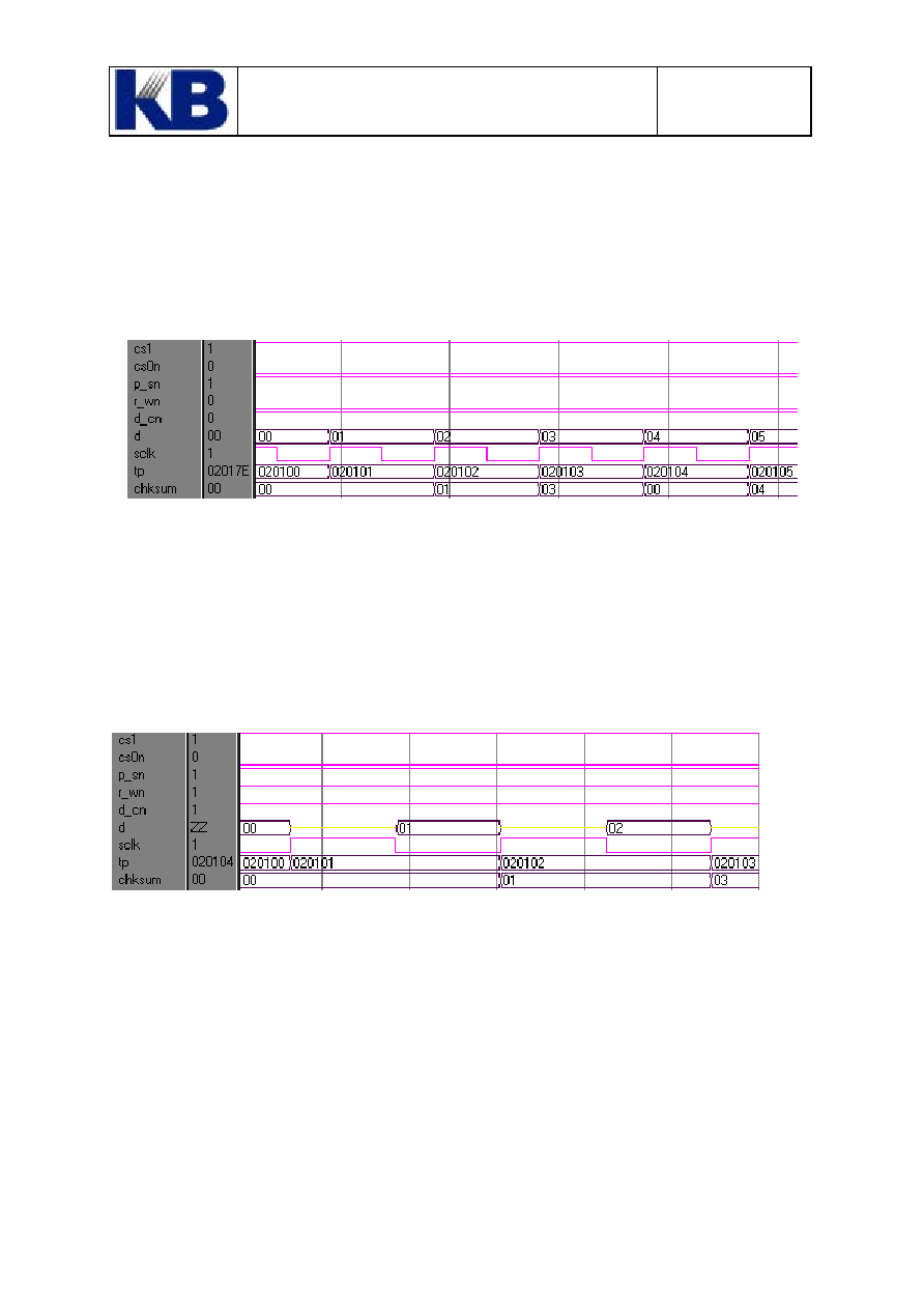
The timing chart below exemplifies when original TP is 0x02017f, then 0x00, 0x01, 0x02
was written sequentially to TPL, TPH, then TPP, the TP becomes 0x020100.
Command Mode SRAM HF88S05
-7- 02/07/01
7.2. Parallel Write Data Mode
To write data to SRAM in parallel mode, assert Strobe in Data Write Mode (D_Cn @ Vih and
R_Wn at Vil). The checksum register will be updated, and the TP register will be incremented
at the rising edge of Strobe signal.
7.3. Parallel Read Data Mode
To Read from SRAM in parallel mode, assert the Strobe in Read Data mode (R_Wn at high
and D_Cn low). The data will appear on the Data bus after proper access time. The TP
will increment and Checksum will update at the rising edge of Strobe. Register select will
be reset by Read Data operation.
7.4. Parallel Read Checksum Mode
To read the checksum result from previous data transfer (either from SRAM or to SRAM),
assert the Strobe signal in Read Command mode (R_Wn is high and D_Cn low).

Command Mode SRAM HF88S05
-8- 02/07/01
8. Serial Mode
The serial interface is preferable to parallel interface in applications where I/O pins are
limited. The interface logic circuit is basically the same as the parallel mode except that an
internal shift register and bit counter are used to facilitate transferring serial data from/to
external MCU.
Multiple devices array can also be used in serial mode. The chip array is connected in daisy
chain manner. The MCU's serial data output pin drives the SDI pin of the first device.
The SDO pin of the device then, in turn, drives the SDI pin of the next device in the chain.
The SDO pin of the last device then connects back to the MCU's SDI pin to complete the
loop.
There could be only one active device in the array at one time, while the other device must be
deselected.
8.1. Bi-directional Synchronous Serial Data Interface
The Serial interface is a Bi-directional Synchronous Serial Interface. The Serial Data can be
written to Registers (such as TPL, TPH, TPP registers) as well as SRAM through the serial
interface. The Checksum and SRAM contents can also be read through Serial Interface, too.
The Serial Data Input SDI pin is connected to LSB of internal shift register. With each
rising edge of SCLK pin, the SDI input is shifted into the shift register. At the eighth rising
edge of SCLK, the content of shift Register is transferred from/to registers or SRAM
depending on the status of D_Cn and R_Wn.
If R_Wn is at "high" state at the eighth rising edge of SCLK then either the contents of

Command Mode SRAM HF88S05
-9- 02/07/01
Checksum Register (if D_Cn is "low") or SRAM been addressed (if D_Cn is "high") will be
latched into the internal shift register. Then the contents of Shift Register can be shifted out
with the next eight rising edges of SCLK.
So one thing important should be noted here when using the Serial Data Interface to read
checksum register or SRAM data is that one dummy read should be performed before the real
data can be shifted out from SDO pin.
8.2. Serial Write Command Mode
The sequence of setting up addresses for data transfer is similar to the parallel mode. The
register pointer will be reset by accesses to SRAM data in the same way as the parallel mode
does. So immediately after completion of previous data transfers or when the device is just
selected, the command writes will be made to TPL, TPH then TPP registers and then wrap
around. If unsure any time during the transfer, a dummy data read can be made to reset the
register select.
8.3. Serial Write Data Mode
With each rising edge of SCLK signal in the serial data write mode (P_Sn @ logic `0', R_Wn
@ logic `0', and D_Cn @ logic `1'), the Data on the SDI pin will be shifted into the internal
shift register. The content of less significant 7 Bits of the internal shift register along with
SDI pin will be transfer to SRAM at the eighth rising edge of SCLK. The checksum register
will be updated, and the TP register will be incremented. The status of R_Wn, D_Cn and
SDI must be held steady in the mean time.

Command Mode SRAM HF88S05
-10- 02/07/01
8.4. Serial Read Data Mode
If both R_Wn, and D_Cn are at high level at the eighth rising edge of SCLK then the contents
of SRAM been addressed will be latched into the internal shift register. Then the contents
of shift register can be shifted out with the next eight rising edges of SCLK.
So one thing important should be noted here when using the Serial Data Interface to read
SRAM data is that one dummy read should be performed before the real data can be shifted
out from SDO pin.
8.5. Serial Read Checksum Mode
Reading checksum in serial mode is similar to Read data mode except that the D_Cn is at low
level instead of high.

Command Mode SRAM HF88S05
-11- 02/07/01
9. Power consideration
In order to conserve power consumed by the device, the static power consumption by SRAM
Sense Amplifier need to be minimized. Since the Sense Amplifier is on whenever the device
is selected and Strobe/SCLK is asserted low in Data Read Mode. Therefore the way to save
power is to minimize the duty of the overall Strobe/SCLK signal to an extent that it is just
long enough to satisfy the access time so that the static power consumption can be lowered.
10. Absolute Maximum Rating
Items Symbol
Rating
Condition
Supply Voltage
V
DD
-0.3 to 6 V
Input Voltage
V
IN
-0.3 to Vdd+0.3 V
Operating Temperature
T
OPR
-0 to 70
∞C
Storage Temperature
T
STR
-55 to 125
∞C
11. AC Electrical Characteristics
READ CYCLE
VCC=5V±0.5V VCC=2.7V±0.3V
Unit
Item
Symbol
Min Max Min Max
Access
Time
tacc TBD TBD
ns

Command Mode SRAM HF88S05
-12- 02/07/01
12. Electrical Characteristics
(VSS = 0V, VDD = 5.0 V, TOPR = 25
∞C unless otherwise noted)
Parameter Sym.
Min.
Typ.
Max
Unit
Condition
Supply
Voltage
VDD
2.4 - 5.5 V
Operating
Current
IDD
- TBD
- mA
No
load
Standby Current
IDD
-
10
-
µA
No load
Input voltage
VIH
VIL
0.7
0
-
-
1
0.3
VDD
VDD = 4V ~ 6V
Input current leakage
IIL
-
-
+/- 10
µA
13. Application Circuit
The application circuit diagram shows one of the KB's MCU uses two HF88S05 as expansion
RAMs. Please note that the SDO pin of the first device drive SDI pin of the second device
and only one device select pin DEV1 is used to select between one of the two device. The
P_Sn pins are tied to ground operate at serial mode.

Command Mode SRAM HF88S05
-13- 02/07/01
LCD Panel
LCDPANEL
CO
M
[
7..0]
SEG
[23..0]
Phone Interface
PHONE
T
R
DTMFO
KTONE
OFFHK
AVDD
AVDD
AVDD
VDD
VDD
VDD
VDD
AGND
AGND
AGND
VDD
VDD
DTMFO
KTONE
SEG0
SEG1
OFFHK
SEG2
SEG3
VTDET
SEG4
DTMFO
SEG5
KTONE
SEG6
PC7
SEG7
PC6
SEG8
PC5
SEG9
PC4
SEG10
PC3
SEG11
PC2
SEG12
PC1
SEG13
PC0
SEG14
RST
SEG15
SEG16
SEG17
DEV1
SEG18
SDO
D
EV1
SEG19
D_Cn
D_Cn
SDI
SEG20
R_Wn
SCLK
R_Wn
SCLK
SEG21
SEG22
SEG23
P150
T
T
IP
P151
P152
R
R
ING
P
153
P150
P151
P152
P153
P154
P155
P156
RNGDET
P170
P171
P172
P173
P174
OPO
RNGDET
OPIP
OPIN
P177
P176
P175
P174
P173
P172
P171
P170
COM0
P157
COM1
P156
COM2
P155
COM3
P154
COM4
COM5
COM6
COM7
F1
FUSE
250V/0.25A
RV1
250V
D1
1N4148
2
1
D2
1N4148
2
1
R1
470K
J1
RJ11C
1
2
4
3
D3
1N4004
2
1
D4
1N4004
2
1
D5
1N4004
2
1
D6
1N4004
2
1
L1
100uH
L2
100uH
D7
1N4148
2
1
D8
1N4148
2
1
D9
1N4148
2
1
R2
33K
C5
104/250V
R9
430K
C2
104
D10
1N4148
2
1
D11
1N4148
2
1
D12
1N4148
2
1
D13
1N4148
2
1
D14
1N4148
2
1
D15
1N4148
2
1
D16
1N4148
2
1
R3
560K
R4
560K
R5
560K
R6
560K
R7
560K
C13
104
K1
K2
K3
K4
K5
K6
K7
K8
K9
K10
K11
K12
K13
K14
K15
K16
K17
K18
K19
K20
K21
K22
K23
K24
K25
K26
K27
K28
K29
K30
K31
K32
K33
K34
K35
C3
33p
C4
33p
Y1
32768
C6
104/250V
C7
472/250V
C8
472/250V
C11
103
C12
104
R10
430K
R11
34K
+
C10
0.22uF
R14
270K
R18
100K
R12
34K
C16
104
C9
104
R13
53.6K
R15
464K
+
C1
0.22uF
R8
270K
R17
60K
C17
104
C18
104
C19
104
U1
KB88A42
57
52
53
54
56
60
29
30
31
32
33
34
35
36
37
38
39
40
41
42
43
44
45
46
47
48
49
50
51
15
14
6
23
22
17
16
11
12
13
18
19
20
21
24
25
58
5
7
8
9
10
1
2
3
4
61
62
63
81
64
65
66
67
68
69
71
72
73
74
75
76
77
78
79
80
59
87
86
85
84
83
82
55
28
26
27
70
LV2
COM0
LC1
LC2
LV1
GND
S15
S14
S13
S12
S11
S10
S9
S8
S7
S6
S5
S4
S3
S2
S1
S0
COM7
COM6
COM5
COM4
COM3
COM2
COM1
S29/P155
S30/P156
S38/P176
S21/P145
S22/P146
S27/P153
S28/P154
S33/P171
S32/P170
S31/P157
S26/P152
S25/P151
S24/P150
S23/P147
S20/P144
S19/P143
LV3
S39/P177
S37/P175
S36/P174
S35/P173
S34/P172
CAP1
CAP2
RNGDI
RNGRC
OPIN
OPIP
OPO
RSTP
FXO
FXI
TSTP
SXO
SXI
VDD
DTMFO
KEYTONE
PRTC7
PRTC6
PRTC5
PRTC4
PRTC3
PRTC2
PRTC1
PRTC0
LV4
INP
INN
GCFB
VREF
VSSA
VDDA
LVF
S16/P140
S18/P142
S17/P141
VDTR
HF88S05
13
11
10
18
5
15
16
12
9
8
7
6
1
4
14
17
3
2
D7
D5
D4
VDD
R_WN
SDI
SDO
D6
D3
D2
D1
D0
P_SN
D_CN
SCLK
CS1
CS0N
VSS
C15
18p
C14
18p
Y2
3579545Hz
R16
60.4K
HF88S05
13
11
10
18
5
15
16
12
9
8
7
6
1
4
14
17
3
2
D7
D5
D4
VDD
R_WN
SDI
SDO
D6
D3
D2
D1
D0
P_SN
D_CN
SCLK
CS1
CS0N
VSS
LINE
Ring detector
12
3
45
6
78
9
0#
*
UP
DOWN
Erase
Option
Dial
Auto
Flash
HF
HOLD
M1
M2
M3
M4
M5
Redial
Pause
Mute
PGM
M6
M7
M8
M9
M10
High Pot! Keep Clearance!
RNGRC