SPEC NO: DSAA4049
REV NO: V.1
DATE: SEP/21/2001
PAGE: 1 OF 4
Description
The High Efficiency Red source color devices are
made with Gallium Arsenide Phosphide on Gallium
Phosphide Orange Light Emitting Diode.
2.0x1.2mm SMD CHIP LED LAMP
AP2012EC HIGH EFFICIENCY RED
Notes:
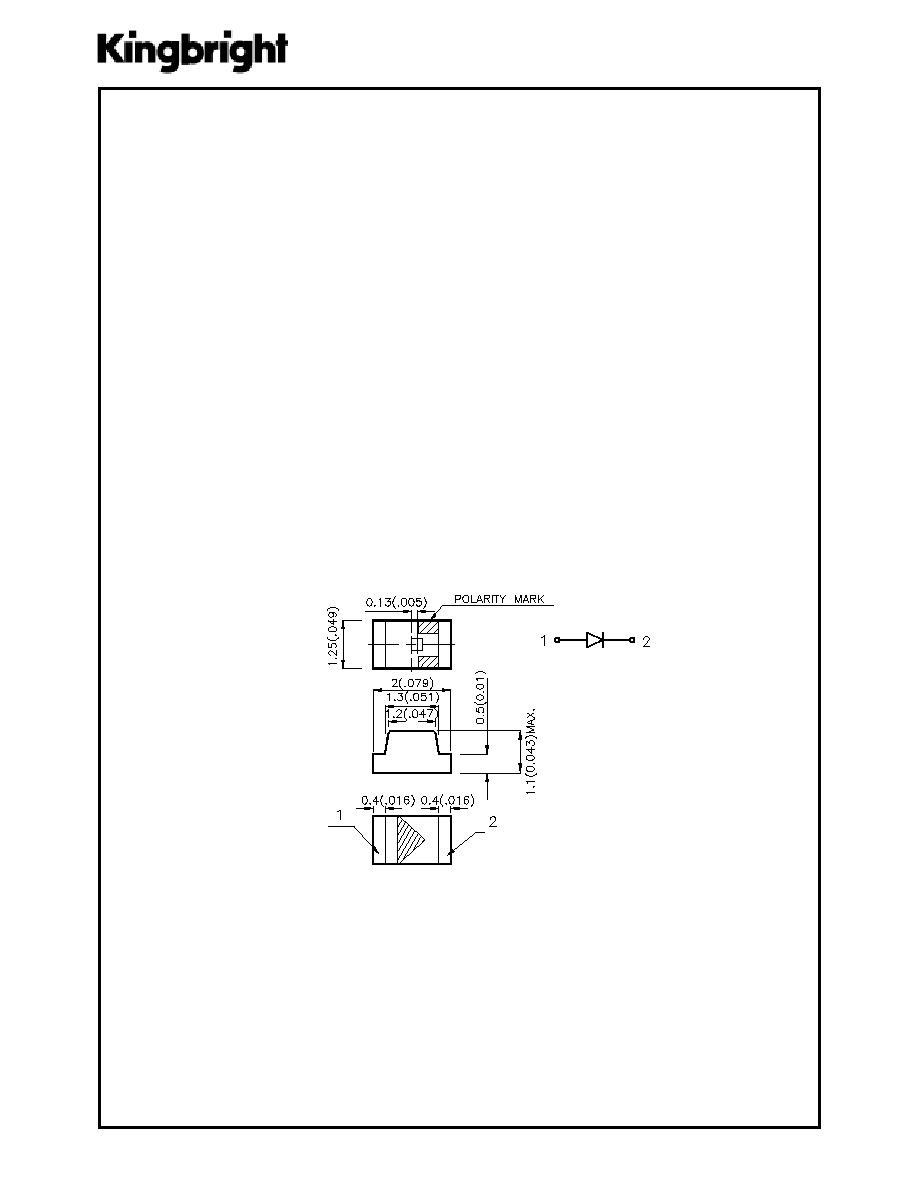
1. All dimensions are in millimeters (inches).
2. Tolerance is
±
0.1(0.004") unless otherwise noted.
3. Lead spacing is measured where the lead emerge package.
4. Specifications are subject to change without notice.
Features
!
2.0mmx1.2mm SMT LED, 1.1mm THICKNESS.
!
LOW POWER CONSUMPTION.
!
WIDE VIEWING ANGLE.
!
IDEAL FOR BACKLIGHT AND INDICATOR.
!
VARIOUS COLORS AND LENS TYPES AVAILABLE.
!
PACKAGE : 2000PCS / REEL.
Package Dimensions
SPEC NO: DSAA4049
REV NO: V.1
DATE: SEP/21/2001
PAGE: 2 OF 4
Electrical / Optical Characteristics at T
)
=25
°°
°°
°
C
Absolute Maximum Ratings at T
)
=25
°°
°°
°
C
Note:
1. 1/10 Duty Cycle, 0.1ms Pulse Width.
Selection Guide
Note:
1.
1/2 is the angle from optical centerline where the luminous intensity is 1/2 the optical centerline value.
.
o
N
t
r
a
P
.
o
N
t
r
a
P
.
o
N
t
r
a
P
.
o
N
t
r
a
P
.
o
N
t
r
a
P
e
c
i
D e
c
i
D e
c
i
D e
c
i
D e
c
i
D
e
p
y
T
s
n
e
L
e
p
y
T
s
n
e
L
e
p
y
T
s
n
e
L
e
p
y
T
s
n
e
L
e
p
y
T
s
n
e
L
)
d
c
m
(
v
I
)
d
c
m
(
v
I
)
d
c
m
(
v
I
)
d
c
m
(
v
I
)
d
c
m
(
v
I
A
m
0
2
@
g
n
i
w
e
i
V
g
n
i
w
e
i
V
g
n
i
w
e
i
V
g
n
i
w
e
i
V
g
n
i
w
e
i
V
e
l
g
n
A
.
n
i
M .
n
i
M .
n
i
M .
n
i
M .
n
i
M
.
p
y
T .
p
y
T .
p
y
T .
p
y
T .
p
y
T
2
/
1
2 2
/
1
2 2
/
1
2 2
/
1
2 2
/
1
2
C
E
2
1
0
2
P
A
)
P
a
G
/
P
s
A
a
G
(
D
E
R
Y
C
N
E
I
C
I
F
F
E
H
G
I
H
R
A
E
L
C
R
E
T
A
W
5
2
1
°
0
2
1
l
o
b
m
y
S
l
o
b
m
y
S
l
o
b
m
y
S
l
o
b
m
y
S
l
o
b
m
y
S
r
e
t
e
m
a
r
a
P
r
e
t
e
m
a
r
a
P
r
e
t
e
m
a
r
a
P
r
e
t
e
m
a
r
a
P
r
e
t
e
m
a
r
a
P
e
c
i
v
e
D
e
c
i
v
e
D
e
c
i
v
e
D
e
c
i
v
e
D
e
c
i
v
e
D
.
p
y
T .
p
y
T .
p
y
T .
p
y
T .
p
y
T
.
x
a
M .
x
a
M .
x
a
M .
x
a
M .
x
a
M
s
ti
n
U s
ti
n
U s
ti
n
U s
ti
n
U s
ti
n
U
s
n
o
it
i
d
n
o
C
t
s
e
T
s
n
o
it
i
d
n
o
C
t
s
e
T
s
n
o
it
i
d
n
o
C
t
s
e
T
s
n
o
it
i
d
n
o
C
t
s
e
T
s
n
o
it
i
d
n
o
C
t
s
e
T
k
a
e
p
h
t
g
n
e
l
e
v
a
W
k
a
e
P
d
e
R
y
c
n
e
i
c
if
f
E
h
g
i
H
7
2
6
m
n
A
m
0
2
=
F
I
D
h
t
g
n
e
l
e
v
a
W
e
t
a
n
i
m
o
D
d
e
R
y
c
n
e
i
c
if
f
E
h
g
i
H
5
2
6
m
n
A
m
0
2
=
F
I
2
/
1
h
t
d
i
w
fl
a
H
e
n
i
L
l
a
rt
c
e
p
S
d
e
R
y
c
n
e
i
c
if
f
E
h
g
i
H
5
4
m
n
A
m
0
2
=
F
I
C
e
c
n
a
ti
c
a
p
a
C
d
e
R
y
c
n
e
i
c
if
f
E
h
g
i
H
5
1
F
p
z
H
M
1
=
f;
V
0
=
F
V
V
F
e
g
a
tl
o
V
d
r
a
w
r
o
F
d
e
R
y
c
n
e
i
c
if
f
E
h
g
i
H
0
.
2
5
.
2
V
A
m
0
2
=
F
I
I
R
t
n
e
rr
u
C
e
s
r
e
v
e
R
d
e
R
y
c
n
e
i
c
if
f
E
h
g
i
H
0
1
A
u
V
5
=
R
V
r
e
t
e
m
a
r
a
P
r
e
t
e
m
a
r
a
P
r
e
t
e
m
a
r
a
P
r
e
t
e
m
a
r
a
P
r
e
t
e
m
a
r
a
P
d
e
r
y
c
n
e
i
c
if
f
E
h
g
i
H
d
e
r
y
c
n
e
i
c
if
f
E
h
g
i
H
d
e
r
y
c
n
e
i
c
if
f
E
h
g
i
H
d
e
r
y
c
n
e
i
c
if
f
E
h
g
i
H
d
e
r
y
c
n
e
i
c
if
f
E
h
g
i
H
s
ti
n
U s
ti
n
U s
ti
n
U s
ti
n
U s
ti
n
U
n
o
it
a
p
i
s
s
i
d
r
e
w
o
P
5
0
1
W
m
t
n
e
rr
u
C
d
r
a
w
r
o
F
C
D
0
3
A
m
]
1
[
t
n
e
rr
u
C
d
r
a
w
r
o
F
k
a
e
P
0
6
1
A
m
e
g
a
tl
o
V
e
s
r
e
v
e
R
5
V
e
r
u
t
a
r
e
p
m
e
T
g
n
it
a
r
e
p
O
0
4
-
°
5
8
+
o
T
C
°
C
e
r
u
t
a
r
e
p
m
e
T
e
g
a
r
o
t
S
0
4
-
°
5
8
+
o
T
C
°
C
SPEC NO: DSAA4049
REV NO: V.1
DATE: SEP/21/2001
PAGE: 4 OF 4
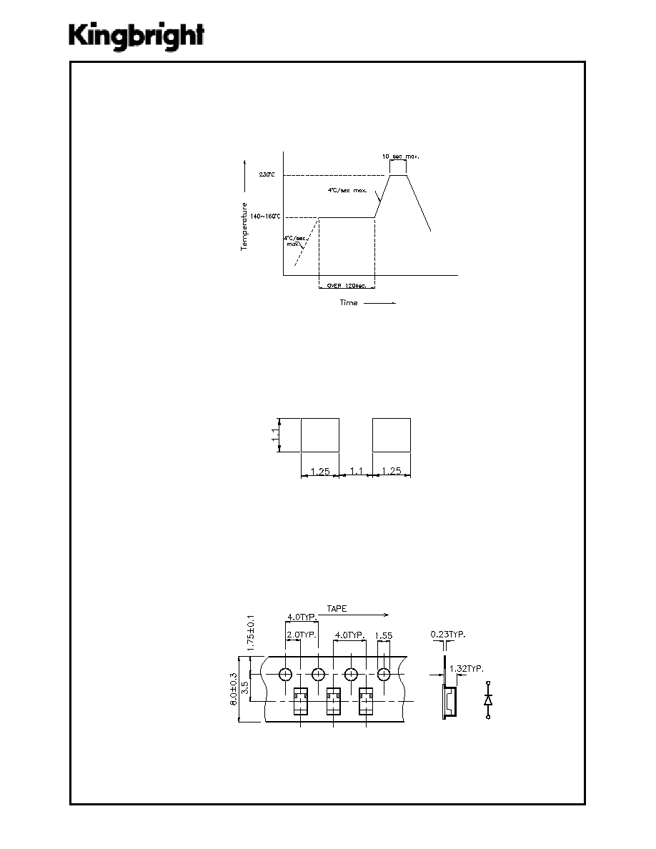
Recommended Soldering Pattern
(Units : mm)
Tape Specifications
(Units : mm)
AP2012EC
SMT Reflow Soldering Instructions
Number of reflow process shall be less than 2 times and cooling
process to normal temperature is required between first and
second soldering process.