SPEC NO: DSAD0942
REV NO: V.1
DATE:MAR/18/2003
PAGE: 1 OF 4
APPROVED : J. Lu
CHECKED : Allen Liu
DRAWN:D.L.HUANG
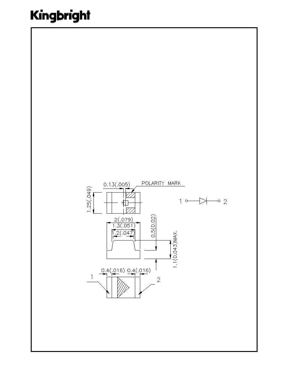
2.0x1.25mm SMD CHIP LED LAMP
AP2012MBC BLUE
Notes:
1. All dimensions are in millimeters (inches).
2. Tolerance is
±
0.1(0.004") unless otherwise noted.
3. Specifications are subject to change without notice.
Package Dimensions
Description
The Blue source color devices are made with GaN
on SiC Light Emitting Diode.
Static electricity and surge damage the LEDS. It is
recommended to use a wrist band or anti-
electrostatic glove when handling the LEDs.
All devices, equipment and machinery must be
electrically grounded.
Features
!
2.0mmx1.25mm SMT LED, 1.1mm THICKNESS.
!
LOW POWER CONSUMPTION.
!
WIDE VIEWING ANGLE.
!
IDEAL FOR BACKLIGHT AND INDICATOR.
!
VARIOUS COLORS AND LENS TYPES AVAILABLE.
!
PACKAGE : 2000PCS / REEL.
SPEC NO: DSAD0942
REV NO: V.1
DATE:MAR/18/2003
PAGE: 2 OF 4
APPROVED : J. Lu
CHECKED : Allen Liu
DRAWN:D.L.HUANG
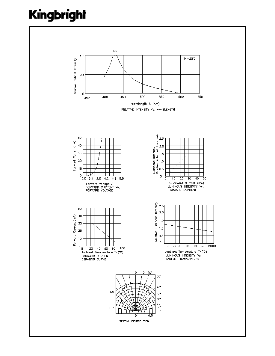
Selection Guide
Note:
1.
1/2 is the angle from optical centerline where the luminous intensity is 1/2 the optical centerline value.
Absolute Maximum Ratings at T
)
=25
°°
°°
°
C
Note:
1. 1/10 Duty Cycle, 0.1ms Pulse Width.
Electrical / Optical Characteristics at T
)
=25
°°
°°
°
C
.
o
N
t
r
a
P
.
o
N
t
r
a
P
.
o
N
t
r
a
P
.
o
N
t
r
a
P
.
o
N
t
r
a
P
e
c
i
D e
c
i
D e
c
i
D e
c
i
D e
c
i
D
e
p
y
T
s
n
e
L
e
p
y
T
s
n
e
L
e
p
y
T
s
n
e
L
e
p
y
T
s
n
e
L
e
p
y
T
s
n
e
L
)
d
c
m
(
v
I
)
d
c
m
(
v
I
)
d
c
m
(
v
I
)
d
c
m
(
v
I
)
d
c
m
(
v
I
A
m
0
2
@
g
n
i
w
e
i
V
g
n
i
w
e
i
V
g
n
i
w
e
i
V
g
n
i
w
e
i
V
g
n
i
w
e
i
V
e
l
g
n
A
.
n
i
M .
n
i
M .
n
i
M .
n
i
M .
n
i
M
.
p
y
T .
p
y
T .
p
y
T .
p
y
T .
p
y
T
2
/
1
2 2
/
1
2 2
/
1
2 2
/
1
2 2
/
1
2
C
B
M
2
1
0
2
P
A
)
N
a
G
(
E
U
L
B
R
A
E
L
C
R
E
T
A
W
4
0
1
°
0
2
1
l
o
b
m
y
S
l
o
b
m
y
S
l
o
b
m
y
S
l
o
b
m
y
S
l
o
b
m
y
S
r
e
t
e
m
a
r
a
P
r
e
t
e
m
a
r
a
P
r
e
t
e
m
a
r
a
P
r
e
t
e
m
a
r
a
P
r
e
t
e
m
a
r
a
P
e
c
i
v
e
D
e
c
i
v
e
D
e
c
i
v
e
D
e
c
i
v
e
D
e
c
i
v
e
D
.
p
y
T .
p
y
T .
p
y
T .
p
y
T .
p
y
T
.
x
a
M .
x
a
M .
x
a
M .
x
a
M .
x
a
M
s
ti
n
U s
ti
n
U s
ti
n
U s
ti
n
U s
ti
n
U
s
n
o
it
i
d
n
o
C
t
s
e
T
s
n
o
it
i
d
n
o
C
t
s
e
T
s
n
o
it
i
d
n
o
C
t
s
e
T
s
n
o
it
i
d
n
o
C
t
s
e
T
s
n
o
it
i
d
n
o
C
t
s
e
T
k
a
e
p
h
t
g
n
e
l
e
v
a
W
k
a
e
P
e
u
l
B
0
3
4
m
n
I
F
A
m
0
2
=
D
h
t
g
n
e
l
e
v
a
W
e
t
a
n
i
m
o
D
e
u
l
B
6
6
4
m
n
I
F
A
m
0
2
=
2
/
1
h
t
d
i
w
-f
l
a
H
e
n
i
L
l
a
rt
c
e
p
S
e
u
l
B
0
6
m
n
I
F
A
m
0
2
=
C
e
c
n
a
ti
c
a
p
a
C
e
u
l
B
0
0
1
F
p
V
F
z
H
M
1
=
f;
V
0
=
V
F
e
g
a
tl
o
V
d
r
a
w
r
o
F
e
u
l
B
8
.
3
5
.
4
V
I
F
A
m
0
2
=
I
R
t
n
e
rr
u
C
e
s
r
e
v
e
R
e
u
l
B
0
1
A
u
V
R
V
5
=
r
e
t
e
m
a
r
a
P
r
e
t
e
m
a
r
a
P
r
e
t
e
m
a
r
a
P
r
e
t
e
m
a
r
a
P
r
e
t
e
m
a
r
a
P
e
u
l
B e
u
l
B e
u
l
B e
u
l
B e
u
l
B
s
ti
n
U s
ti
n
U s
ti
n
U s
ti
n
U s
ti
n
U
n
o
it
a
p
i
s
s
i
d
r
e
w
o
P
5
0
1
W
m
t
n
e
r
r
u
C
d
r
a
w
r
o
F
C
D
0
3
A
m
]
1
[
t
n
e
r
r
u
C
d
r
a
w
r
o
F
k
a
e
P
0
5
1
A
m
e
g
a
tl
o
V
e
s
r
e
v
e
R
5
V
e
r
u
t
a
r
e
p
m
e
T
e
g
a
r
o
t
S
/
g
n
it
a
r
e
p
O
0
4
-
°
5
8
+
o
T
C
°
C
SPEC NO: DSAD0942
REV NO: V.1
DATE:MAR/18/2003
PAGE: 4 OF 4
APPROVED : J. Lu
CHECKED : Allen Liu
DRAWN:D.L.HUANG
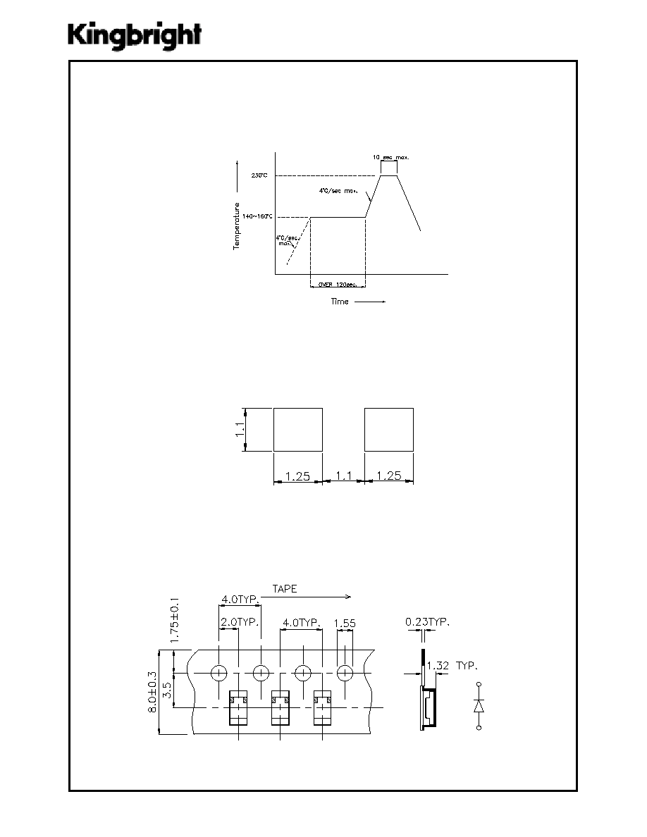
Recommended Soldering Pattern
(Units : mm)
Tape Specifications
(Units : mm)
AP2012MBC
SMT Reflow Soldering Instructions
Number of reflow process shall be less than 2 times and cooling
process to normal temperature is required between first and
second soldering process.