SPEC NO:DSAD1359
REV NO: V.1
DATE:MAR/31/2003
PAGE: 1 OF 4
APPROVED: J.LU
CHECKED: Allen Liu
DRAWN: L.ZHANG
3.0mmx1.0mm INFRA-RED EMITTING DIODE
Features
!
3.0mm x 1.0mm SMT LED, 2.0mm THICKNESS.
!
LOW POWER CONSUMPTION.
!
WIDE VIEWING ANGLE.
!
IDEAL FOR BACK LIGHT AND INDICATOR.
!
VARIOUS COLORS AND LENS TYPES AVAILABLE.
!
PACKAGE : 2000PCS / REEL.
Package Dimensions
Notes:
1. All dimensions are in millimeters (inches).
2. Tolerance is
±
0.15(0.006") unless otherwise noted.
3. Specifications are subject to change without notice.
APA3010F3C
Description
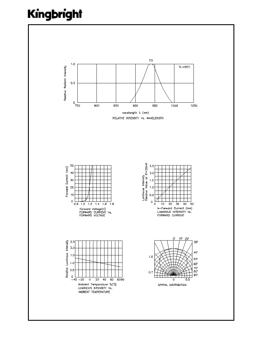
F3 Made with Gallium Arsenide Infrared Emitting
diodes.

SPEC NO:DSAD1359
REV NO: V.1
DATE:MAR/31/2003
PAGE: 2 OF 4
APPROVED: J.LU
CHECKED: Allen Liu
DRAWN: L.ZHANG
Selection Guide
Electrical / Optical Characteristics at T
A
=25
∞∞
∞∞
∞
C
Absolute Maximum Ratings at T
A
=25
∞∞
∞∞
∞
C
Note:
1.
1/2 is the angle from optical centerline where the luminous intensity is 1/2 the optical centerline value.
Note:
1. 1/100 Duty Cycle, 10us Pulse Width.
r
e
t
e
m
a
r
a
P
r
e
t
e
m
a
r
a
P
r
e
t
e
m
a
r
a
P
r
e
t
e
m
a
r
a
P
r
e
t
e
m
a
r
a
P
N
/
P N
/
P N
/
P N
/
P N
/
P
l
o
b
m
y
S
l
o
b
m
y
S
l
o
b
m
y
S
l
o
b
m
y
S
l
o
b
m
y
S
.
p
y
T
.
p
y
T
.
p
y
T
.
p
y
T
.
p
y
T
.
x
a
M .
x
a
M .
x
a
M .
x
a
M
.
x
a
M
ti
n
U ti
n
U ti
n
U ti
n
U ti
n
U
n
o
it
i
d
n
o
C
n
o
it
i
d
n
o
C
n
o
it
i
d
n
o
C
n
o
it
i
d
n
o
C
n
o
it
i
d
n
o
C
e
g
a
tl
o
V
d
r
a
w
r
o
F
3
F
V
F
2
.
1
6
.
1
V
I
F
A
m
0
2
=
t
n
e
r
r
u
C
e
s
r
e
v
e
R
3
F
I
R
-
0
1
A
u
V
R
V
5
=
e
c
n
a
ti
c
a
p
a
C
3
F
C
0
9
-
F
p
V
F
z
H
M
1
=
f
;
V
0
=
h
t
g
n
e
l
e
v
a
W
l
a
r
t
c
e
p
S
k
a
e
P
3
F
P
0
4
9
-
m
n
I
F
A
m
0
2
=
h
t
d
i
w
d
n
a
B
l
a
r
t
c
e
p
S
3
F
2
/
1
0
5
-
m
n
I
F
A
m
0
2
=
.
o
N
t
r
a
P
.
o
N
t
r
a
P
.
o
N
t
r
a
P
.
o
N
t
r
a
P
.
o
N
t
r
a
P
e
c
i
D e
c
i
D e
c
i
D e
c
i
D e
c
i
D
e
p
y
T
s
n
e
L
e
p
y
T
s
n
e
L
e
p
y
T
s
n
e
L
e
p
y
T
s
n
e
L
e
p
y
T
s
n
e
L
)
r
s
/
W
m
(
o
P
)
r
s
/
W
m
(
o
P
)
r
s
/
W
m
(
o
P
)
r
s
/
W
m
(
o
P
)
r
s
/
W
m
(
o
P
A
m
0
2
@
g
n
i
w
e
i
V
g
n
i
w
e
i
V
g
n
i
w
e
i
V
g
n
i
w
e
i
V
g
n
i
w
e
i
V
e
l
g
n
A
.
n
i
M .
n
i
M .
n
i
M .
n
i
M .
n
i
M
.
p
y
T .
p
y
T
.
p
y
T
.
p
y
T
.
p
y
T
2
2
2
2
2
2
/
1 2
/
1 2
/
1 2
/
1 2
/
1
C
3
F
0
1
0
3
A
P
A
s
A
a
G
R
A
E
L
C
R
E
T
A
W
4
.
0
2
.
1
0
2
1
∞
r
e
t
e
m
a
r
a
P
r
e
t
e
m
a
r
a
P
r
e
t
e
m
a
r
a
P
r
e
t
e
m
a
r
a
P
r
e
t
e
m
a
r
a
P
l
o
b
m
y
S
l
o
b
m
y
S
l
o
b
m
y
S
l
o
b
m
y
S
l
o
b
m
y
S
3
F3
F3
F3
F3
F
s
ti
n
U
s
ti
n
U
s
ti
n
U
s
ti
n
U
s
ti
n
U
n
o
it
a
p
i
s
s
i
D
r
e
w
o
P
P
T
0
0
1
W
m
t
n
e
r
r
u
C
d
r
a
w
r
o
F
I
F
0
5
A
m
]
1
[t
n
e
r
r
u
C
d
r
a
w
r
o
F
k
a
e
P
i
S
F
2
.
1
A
e
g
a
tl
o
V
e
s
r
e
v
e
R
V
R
5
V
e
r
u
t
a
r
e
p
m
e
T
g
n
it
a
r
e
p
O
T
A
5
8
+
~
0
4
-
∞
C
e
r
u
t
a
r
e
p
m
e
T
e
g
a
r
o
t
S
T
G
T
S
5
8
+
~
0
4
-
∞
C

SPEC NO:DSAD1359
REV NO: V.1
DATE:MAR/31/2003
PAGE: 4 OF 4
APPROVED: J.LU
CHECKED: Allen Liu
DRAWN: L.ZHANG
Recommended Soldering Pattern
(Units : mm)
Tape Specifications
(Units : mm)
APA3010F3C
SMT Reflow Soldering Instructions
Number of reflow process shall be less than 2 times and cooling
process to normal temperature is required between first and
second soldering process.