SPEC NO:DSAD1078
REV NO: V.1
DATE:MAR/18/2003 PAGE: 1 OF 4
APPROVED: J.Lu
CHECKED: Allen Liu
DRAWN:Y.H.LI
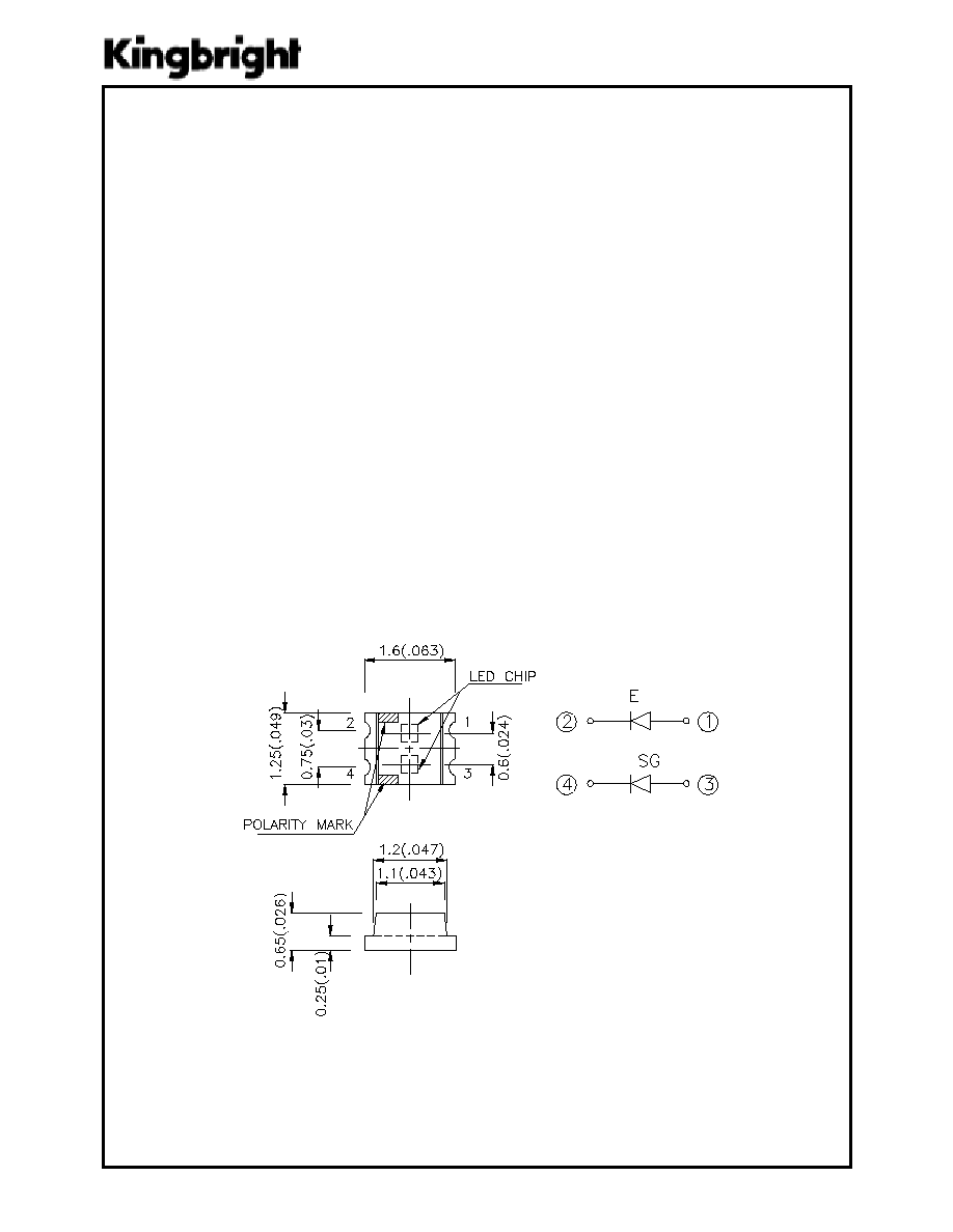
1.6x1.25mm BI-COLOR SMD CHIP LED LAMP
APTB1612ESGC HIGH EFFICIENCY RED
SUPER BRIGHT GREEN
Notes:
1. All dimensions are in millimeters (inches).
2. Tolerance is
±
0.2(0.0079") unless otherwise noted.
3. Specifications are subject to change without notice.
Package Dimensions
Description
The High Efficiency Red source color devices are
made with Gallium Arsenide Phosphide on Gallium
Phosphide Orange Light Emitting Diode.
The Super Bright Green source color devices are
made with Gallium Phosphide Green Light Emitting
Diode.
Features
l
1.6mmx1.25mm SMT LED, 0.65mm THICKNESS.
l
BI -COLOR,LOW POWER CONSUMPTION.
l
WIDE VIEWING ANGLE.
l
IDEAL FOR BACKLIGHT AND INDICATOR.
l
VARIOUS COLORS AND LENS TYPES AVAILABLE.
l
PACKAGE : 2000PCS / REEL.
SPEC NO:DSAD1078
REV NO: V.1
DATE:MAR/18/2003 PAGE: 2 OF 4
APPROVED: J.Lu
CHECKED: Allen Liu
DRAWN:Y.H.LI
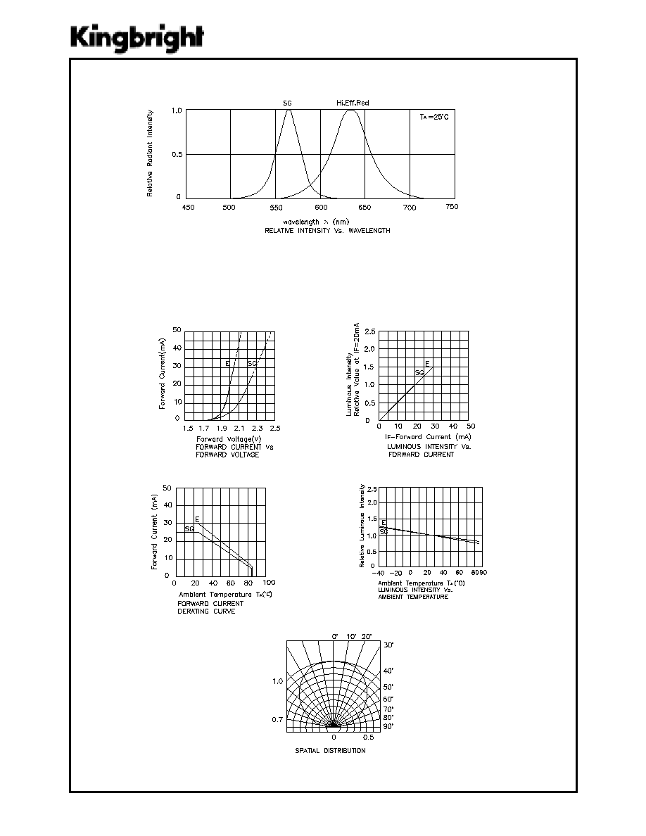
Selection Guide
Electrical / Optical Characteristics at T
A
=25
°°
°°
°
C
Note:
1
.
1/2 is the angle from optical centerline where the luminous intensity is 1/2 the optical centerline value.
Absolute Maximum Ratings at T
A
=25
°°
°°
°
C
Note:
1. 1/10 Duty Cycle, 0.1ms Pulse Width.
lo
b
m
yS lo
b
m
yS lo
b
m
yS lo
b
m
yS lo
b
m
yS
ret
e
m
ar
a
P
ret
e
m
ar
a
P
ret
e
m
ar
a
P
ret
e
m
ar
a
P
ret
e
m
ar
a
P
ec
iv
e
D ec
iv
e
D ec
iv
e
D ec
iv
e
D ec
iv
e
D
.p
yT .p
yT .p
yT .p
yT .p
yT
.x
a
M .x
a
M .x
a
M .x
a
M .x
a
M
sti
n
U sti
n
U sti
n
U sti
n
U sti
n
U
sn
oit
id
no
C
ts
eT
sn
oit
id
no
C
ts
eT
sn
oit
id
no
C
ts
eT
sn
oit
id
no
C
ts
eT
sn
oit
id
no
C
ts
eT
ka
ep
ht
gn
el
ev
a
W
ka
e
P
de
R
yc
ne
icif
fE
hg
iH
ne
er
G
th
gir
B
re
pu
S
72
6 56
5
m
n
I
F
A
m
02
=
D
ht
gn
el
ev
a
W
et
an
im
o
D
de
R
yc
ne
icif
fE
hg
iH
ne
er
G
th
gir
B
re
pu
S
52
6 86
5
m
n
I
F
A
m
02
=
2/
1
ht
di
w-
fla
H
en
iL
lar
tc
ep
S
de
R
yc
ne
icif
fE
hg
iH
ne
er
G
th
gir
B
re
pu
S
54
03
m
n
I
F
A
m
02
=
C
ec
na
tic
ap
a
C
de
R
yc
ne
icif
fE
hg
iH
ne
er
G
th
gir
B
re
pu
S
51
51
F
p
V
F
z
H
M
1=
f;
V
0=
V
F
eg
atl
oV
dr
a
wr
oF
de
R
yc
ne
icif
fE
hg
iH
ne
er
G
th
gir
B
re
pu
S
0.
2 2.
2
5.
2 5.
2
V
I
F
A
m
02
=
I
R
tn
err
u
C
es
re
ve
R
llA
01
A
u
V
R
V
5
=
ret
e
m
ar
a
P
ret
e
m
ar
a
P
ret
e
m
ar
a
P
ret
e
m
ar
a
P
ret
e
m
ar
a
P
de
R
yc
ne
ici
ff
E
hg
iH
de
R
yc
ne
ici
ff
E
hg
iH
de
R
yc
ne
ici
ff
E
hg
iH
de
R
yc
ne
ici
ff
E
hg
iH
de
R
yc
ne
ici
ff
E
hg
iH
ne
er
G
th
gir
B
re
pu
S
ne
er
G
th
gir
B
re
pu
S
ne
er
G
th
gir
B
re
pu
S
ne
er
G
th
gir
B
re
pu
S
ne
er
G
th
gir
B
re
pu
S
sti
n
U sti
n
U sti
n
U sti
n
U sti
n
U
no
ita
pi
ss
id
re
w
o
P
50
1
50
1
W
m
tn
err
u
C
dr
a
wr
oF
C
D
03
52
A
m
]1[
tn
err
u
C
dr
a
wr
oF
ka
e
P
06
1
04
1
A
m
eg
atl
oV
es
re
ve
R
5
5
V
er
ut
ar
ep
m
eT
eg
ar
ot
S/
gn
ita
re
p
O
04
-
°
58
+
oT
C
°
C
.o
N
tra
P
.o
N
tra
P
.o
N
tra
P
.o
N
tra
P
.o
N
tra
P
ec
iD ec
iD ec
iD ec
iD ec
iD
ep
yT
sn
eL
ep
yT
sn
eL
ep
yT
sn
eL
ep
yT
sn
eL
ep
yT
sn
eL
)d
c
m(
vI
)d
c
m(
vI
)d
c
m(
vI
)d
c
m(
vI
)d
c
m(
vI
A
m
02
@
gn
iw
ei
V
gn
iw
ei
V
gn
iw
ei
V
gn
iw
ei
V
gn
iw
ei
V elg
n
A
.ni
M .ni
M .ni
M .ni
M .ni
M
.p
yT .p
yT .p
yT .p
yT .p
yT
2
/
1
2 2
/
1
2 2
/
1
2 2
/
1
2 2
/
1
2
C
G
S
E2
16
1
BT
P
A
)P
a
G/
Ps
Aa
G(
D
E
R
Y
C
N
EI
CI
F
F
E
H
GI
H
R
A
EL
C
R
ET
A
W
4
21
°0
21
)P
a
G(
N
E
E
R
G
T
H
GI
R
B
R
E
P
U
S
6.
2
21
SPEC NO:DSAD1078
REV NO: V.1
DATE:MAR/18/2003 PAGE: 4 OF 4
APPROVED: J.Lu
CHECKED: Allen Liu
DRAWN:Y.H.LI
APTB1612ESGC
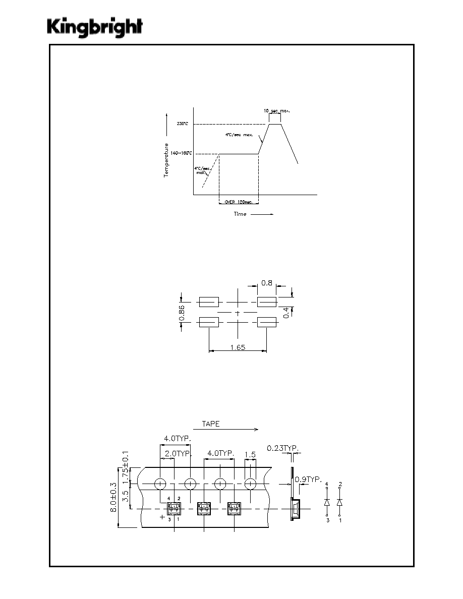
SMT Reflow Soldering Instructions
Recommended Soldering Pattern
(Units : mm)
Tape Specifications
(Units : mm)
Number of reflow process shall be less than 2 times and cooling
process to normal temperature is required between first and
second soldering process.