
SPEC NO:DSAD1568
REV NO: V.1
DATE: APR/19/2003
PAGE: 1 OF 3
APPROVED: J.Lu
CHECKED :Allen Liu
DRAWN: L.ZHANG
ATIR0621DS
PHOTO-INTERRUPTER
Notes:
1. All dimensions are in millimeters (inches).
2. Tolerance is
±
0.25(0.01") unless otherwise noted.
3. Lead spacing is measured where the lead emerge package.
4. Specifications are subject to change without notice.
Features
!
High sensing accuracy
!
High current transfer ratio
!
Both-sides mounting type
Package Dimensions
Absolute Maximum Ratings (T
a
=25
∞∞
∞∞
∞
C)
Applications
!
OA equipment, such as floppy disk drives,
printers, facsimiles, etc
!
VCRs
r
e
t
e
m
a
r
a
P
r
e
t
e
m
a
r
a
P
r
e
t
e
m
a
r
a
P
r
e
t
e
m
a
r
a
P
r
e
t
e
m
a
r
a
P
l
o
b
m
y
S
l
o
b
m
y
S
l
o
b
m
y
S
l
o
b
m
y
S
l
o
b
m
y
S
g
n
it
a
R
g
n
it
a
R
g
n
it
a
R
g
n
it
a
R
g
n
it
a
R
ti
n
U ti
n
U ti
n
U ti
n
U ti
n
U
t
u
p
n
I
t
n
e
r
r
u
c
d
r
a
w
r
o
F
I
F
0
5
A
m
e
g
a
tl
o
v
e
s
r
e
v
e
R
V
R
6
V
n
o
it
a
p
i
s
s
i
d
r
e
w
o
P
P
5
7
W
m
t
u
p
t
u
O
e
g
a
tl
o
v
r
e
tt
i
m
e
-
r
o
t
c
e
ll
o
C
V
O
E
C
5
3
V
e
g
a
tl
o
v
r
o
t
c
e
ll
o
c
-
r
e
tt
i
m
E
V
O
C
E
6
V
t
n
e
r
r
u
c
r
o
t
c
e
ll
o
C
I
C
0
4
A
m
n
o
it
a
p
i
s
s
i
d
r
e
w
o
p
r
o
t
c
e
ll
o
C
P
C
5
7
W
m
e
r
u
t
a
r
e
p
m
e
t
g
n
it
a
r
e
p
O
r
p
o
T
5
8
+
~
5
2
-
∞
C
e
r
u
t
a
r
e
p
m
e
t
e
g
a
r
o
t
S
g
t
s
T
0
0
1
+
~
0
4
-
∞
C
)
s
d
n
o
c
e
s
5
r
o
f
y
d
o
b
m
o
r
f
h
c
n
i
6
1
/
1
(
e
r
u
t
a
r
e
p
m
e
t
g
n
ir
e
d
l
o
S
l
o
s
T
0
6
2
∞
C
SPEC NO:DSAD1568
REV NO: V.1
DATE: APR/19/2003 PAGE: 2 OF 3
APPROVED: J.Lu
CHECKED :Allen Liu
DRAWN: L.ZHANG
Electro-optical Characteristics (T
a
=25
∞∞
∞∞
∞
C)
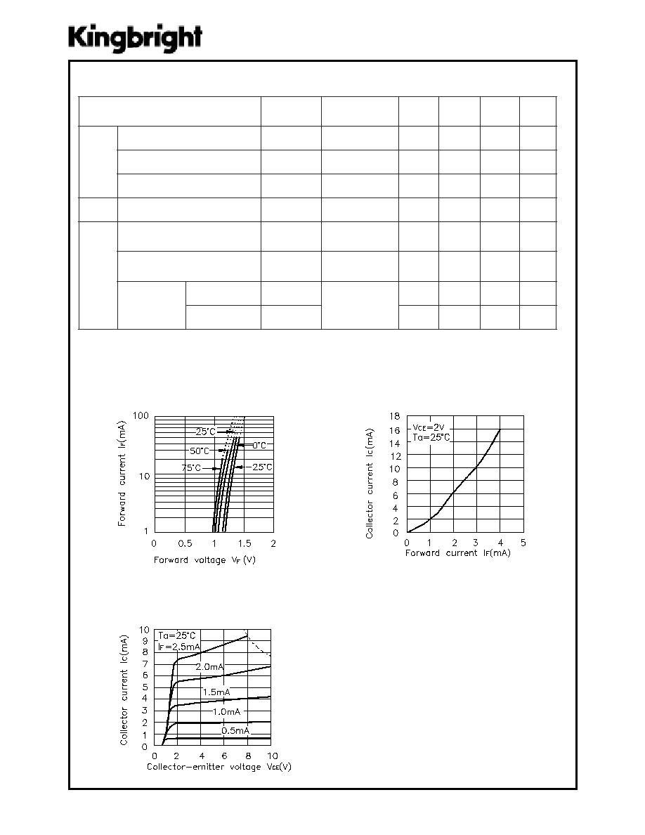
Fig.1 Forward Current vs.
Forward Voltage
Fig.2 Collector Current vs.
Forward Current
Fig.3 Collector Current vs.
Collector-emitter Voltage
r
e
t
e
m
a
r
a
P
r
e
t
e
m
a
r
a
P
r
e
t
e
m
a
r
a
P
r
e
t
e
m
a
r
a
P
r
e
t
e
m
a
r
a
P
l
o
b
m
y
S
l
o
b
m
y
S
l
o
b
m
y
S
l
o
b
m
y
S
l
o
b
m
y
S
s
n
o
it
i
d
n
o
C
s
n
o
it
i
d
n
o
C
s
n
o
it
i
d
n
o
C
s
n
o
it
i
d
n
o
C
s
n
o
it
i
d
n
o
C
.
n
i
M .
n
i
M .
n
i
M .
n
i
M .
n
i
M
.
p
y
T
.
p
y
T
.
p
y
T
.
p
y
T
.
p
y
T
.
x
a
M .
x
a
M .
x
a
M .
x
a
M
.
x
a
M
ti
n
U ti
n
U ti
n
U ti
n
U ti
n
U
t
u
p
n
I
e
g
a
tl
o
v
d
r
a
w
r
o
F
V
F
I
F
A
m
0
2
=
_
2
.
1
5
.
1
V
e
g
a
tl
o
v
d
r
a
w
r
o
f
k
a
e
P
V
M
F
I
M
F
A
5
.
0
=
_
2
4
V
t
n
e
r
r
u
c
e
s
r
e
v
e
R
I
R
V
R
V
5
=
_
_
0
1
µ
A
t
u
p
t
u
O
t
n
e
r
r
u
c
k
r
a
d
r
o
t
c
e
ll
o
C
I
O
E
C
V
E
C
I,
V
0
1
=
F
A
m
0
=
_
_
0
1
6
-
A
r
e
f
s
n
a
r
T
-
t
c
a
r
a
h
c
s
c
it
s
ir
e
o
it
a
r
r
e
f
s
n
a
r
t
t
n
e
r
r
u
C
R
T
C
V
E
C
I,
V
2
=
F
A
m
1
=
_
0
0
2
_
%
e
g
a
tl
o
v
n
o
it
a
r
u
t
a
s
r
e
tt
i
m
e
-
r
o
t
c
e
ll
o
C
V
)
t
a
s
(
E
C
I
F
I,
A
m
2
=
C
A
m
1
=
_
_
0
.
1
V
e
m
it
e
s
n
o
p
s
e
R
e
m
it
e
s
i
R
t
r
V
E
C
I,
V
2
=
C
A
m
0
1
=
R
L
0
0
1
=
_
0
9
0
0
4
µ
c
e
s
e
m
it
ll
a
F
t
f
_
0
8
0
0
3
µ
c
e
s
SPEC NO:DSAD1568
REV NO: V.1
DATE: APR/19/2003
PAGE: 3 OF 3
APPROVED: J.Lu
CHECKED :Allen Liu
DRAWN: L.ZHANG
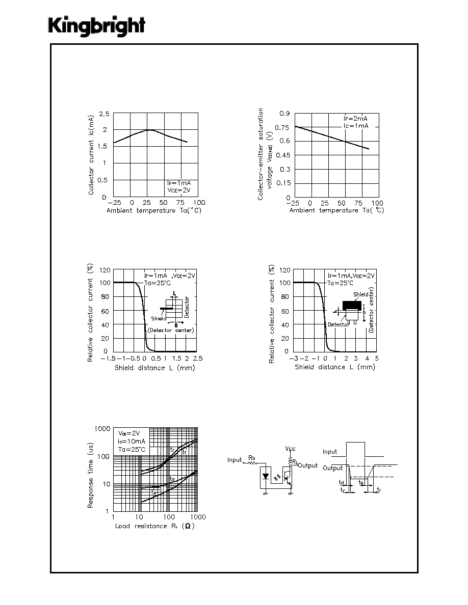
Fig.4 Collector Current vs.
Ambient Temperature
Fig.5 Collector-emitter Saturation
Voltage vs. Ambient Temperature
Fig.6 Relative Collector Current vs.
Shield Distance(1)
Fig.7 Relative Collector Current vs.
Shield Distance(2)
Fig.8 Response Time vs.
Load Resistance
Test Circuit for Response Time