 | –≠–ª–µ–∫—Ç—Ä–æ–Ω–Ω—ã–π –∫–æ–º–ø–æ–Ω–µ–Ω—Ç: KAC-1310 | –°–∫–∞—á–∞—Ç—å:  PDF PDF  ZIP ZIP |

IMAGE SENSOR SOLUTIONS
K A C - 1 3 1 0 R e v . 4 ∑ w w w . k o d a k . c o m / g o / i m a g e r s 5 8 5 - 7 2 2 - 4 3 8 5 E m a i l : i m a g e r s @ k o d a k . c o m
D E V I C E
P E R F O R M A N C E
S P E C I F I C A T I O N
KODAK KAC-1310
Image Sensor
1280 (H) x 1024 (V)
SXGA CMOS Image Sensor
November 7, 2002
Revision 4

IMAGE SENSOR SOLUTIONS
2
IMAGE SENSOR SOLUTIONS
K A C - 1 3 1 0 R e v 4 ∑ w w w . k o d a k . c o m / g o / i m a g e r s 5 8 5 - 7 2 2 - 4 3 8 5 E m a i l : i m a g e r s @ k o d a k . c o m
TABLE OF CONTENTS
TABLE OF FIGURES........................................... 3
LIST OF TABLES................................................. 3
SUMMARY SPECIFICATION .............................. 5
PIN DEFINITIONS................................................ 6
R
ECOMMENDED
H
ARDWARE FOR
KAC-1310
S
ENSOR
E
VALUATION
: ........................................ 7
DEVICE DESCRIPTION....................................... 8
P
IXEL
A
RCHITECTURE
....................................... 10
C
OLOR
F
ILTERS AND
L
ENSLETS
......................... 11
F
RAME
C
APTURE
M
ODES
.................................. 11
C
ONTINUOUS
F
RAME
R
OLLING
S
HUTTER
C
APTURE
M
ODE
(CFRS) ................................................. 11
CFRS V
IDEO
E
NCODED
D
ATA
S
TREAM
............. 12
S
INGLE
F
RAME
R
OLLING
S
HUTTER CAPTURE MODE
(SFRS) ........................................................... 12
W
INDOW OF
I
NTEREST
(WOI) C
ONTROL
............ 12
S
UB
-S
AMPLING
C
ONTROL
(R
ESOLUTION
) .......... 12
V
IRTUAL
F
RAME
(VF)........................................ 13
I
NTEGRATION
T
IME
........................................... 13
CFRS I
NTEGRATION
T
IME
................................. 13
SFRS I
NTEGRATION
T
IME
................................. 14
F
RAME
R
ATE
.................................................... 14
CFRS F
RAME
R
ATE
......................................... 14
SFRS F
RAME
R
ATE
......................................... 15
ANALOG SIGNAL PROCESSING CHAIN..... 16
(ASP).............................................................. 16
F
RAME
R
ATE
C
LAMP
(FRC).............................. 16
C
OLUMN
D
IGITAL
O
FFSET
V
OLTAGE
A
DJUST
(CDOVA) ........................................................ 16
P
ROGRAMMABLE
G
AIN
A
MPLIFIER
(PGA) .......... 17
G
AIN
M
ODES
.................................................... 17
Raw Gain Mode: ........................................ 17
Lin1 Gain Mode:......................................... 17
Lin2 Gain Mode:......................................... 17
W
HITE
B
ALANCE
C
ONTROL
PGA (WB G
AIN
)..... 19
E
XPOSURE
G
AIN
PGA (E
XP
G
AIN
A/B) ............. 20
G
LOBAL
D
IGITAL
O
FFSET
V
OLTAGE
A
DJUST
(GDOVA) ........................................................ 20
A
NALOG TO
D
IGITAL
C
ONVERTER
(ADC) ........... 20
PERFORMANCE................................................ 21
T
EST
C
ONDITIONS
............................................ 21
I
MAGING
P
ERFORMANCE
................................... 21
Q
UANTUM
E
FFICIENCY
...................................... 23
D
YNAMIC
R
ANGE
.............................................. 25
T
EMPORAL
N
OISE
............................................. 25
OPERATION ...................................................... 28
I
NITIALIZATION
(S
TANDBY
M
ODE
)....................... 28
S
TANDBY
M
ODE
............................................... 28
O
UTPUT
T
RISTATE
............................................ 28
R
EADOUT
O
RDER
............................................. 28
R
EADOUT
S
PEED
.............................................. 29
I
NTERNAL
B
IAS
C
URRENT
C
ONTROL
.................. 30
TIMING ............................................................... 31
S
TART OF
R
OW
R
EADOUT
(SOF) ...................... 31
H
ORIZONTAL
D
ATA
S
YNC
(VCLK) ..................... 31
D
ATA
V
ALID
(HCLK)......................................... 31
S
TROBE
S
IGNAL
............................................... 33
Example Timing Summary:........................ 35
I
2
C-COMPATIBLE SERIAL INTERFACE.......... 36
KAC-1310 I
2
C B
US
P
ROTOCOL
........................ 37
START S
IGNAL
................................................ 37
S
LAVE
A
DDRESS
T
RANSMISSION
....................... 37
A
CKNOWLEDGMENT
.......................................... 37
D
ATA
T
RANSFER
.............................................. 37
S
TOP
S
IGNAL
................................................... 37
R
EPEATED
START S
IGNAL
............................... 38
I
2
C B
US
C
LOCKING AND SYNCHRONIZATION
....... 38
R
EGISTER
W
RITE
............................................. 38
R
EGISTER
R
EAD
............................................... 38
REGISTER LIST REFERENCE ......................... 41
DETAILED REGISTER BLOCK ASSIGNMENTS
............................................................................ 44
C
OLOR
G
AIN
R
EGISTERS
00
H
03
H
.................. 44
R
EFERENCE
V
OLTAGE
A
DJUST
R
EGISTERS
(0A
H
,
0B
H
)................................................................. 46
P
OWER
C
ONFIGURATION
R
EGISTERS
(0C
H
) ....... 47
R
ESET
C
ONTROL
R
EGISTER
(0E
H
)..................... 48
E
XPOSURE
G
AIN
A R
EGISTER
(10
H
) .................. 49
T
RISTATE
C
ONTROL
R
EGISTER
(12
H
)................. 49
C
OLUMN
DOVA DC R
EGISTER
(20
H
) ................ 51
E
XPOSURE
G
AIN
B (21
H
) ................................... 52
PGA G
AIN
M
ODE
(22
H
)..................................... 53
ADC DOVA (23
H
)............................................ 54
C
APTURE
M
ODE
C
ONTROL
(40
H
) ....................... 55
S
UB
-
SAMPLE
C
ONTROL
(41
H
) ............................ 56
TRIGGER
AND
STROBE C
ONTROL
R
EGISTER
(42
H
)................................................................ 57
P
ROGRAMMABLE
W
INDOW OF
I
NTEREST
(WOI)
(45
H
-4C
H
)......................................................... 58
I
NTEGRATION
T
IME
C
ONTROL
(4E
H
4F
H
) ........ 61
P
ROGRAMMABLE
V
IRTUAL
F
RAME
(50
H
53
H
) .. 62
SOF
AND
VCLK D
ELAY
R
EGISTERS
(54
H
AND
55
H
)
........................................................................ 64
SOF & VCLK W
IDTH
R
EGISTER
(56
H
) .............. 65
R
EADOUT
D
IRECTION
R
EGISTER
(57
H
)............... 66
I
NTERNAL
T
IMING
C
ONTROL
R
EGISTERS
(5F
H
AND
60
H
) ................................................................. 67
C
LAMP
C
ONTROL AND
HCLK D
ELAY
R
EGISTER
(64
H
)................................................................ 68
E
NCODED
S
YNC
R
EGISTER
(65
H
)...................... 69
M
OD
64 C
OLUMN
O
FFSET
C
ORRECTION
R
EGISTER
(80
H
-BF
H
)......................................................... 70
STORAGE AND HANDLING ............................. 71
MECHANICAL DRAWINGS .............................. 73

IMAGE SENSOR SOLUTIONS
3
IMAGE SENSOR SOLUTIONS
K A C - 1 3 1 0 R e v 4 ∑ w w w . k o d a k . c o m / g o / i m a g e r s 5 8 5 - 7 2 2 - 4 3 8 5 E m a i l : i m a g e r s @ k o d a k . c o m
QUALITY ASSURANCE AND RELIABILITY.... 75
ORDERING INFORMATION.............................. 76
A
VAILABLE
P
ART
C
ONFIGURATIONS
................... 76
TABLE OF FIGURES
Figure 1. Pinout Diagram...................................... 6
Figure 2: KAC-1310 Pin Connection Schematic .. 7
Figure 3: KAC-1310 Block Diagram ..................... 8
Figure 4: Optional Bayer RGB Pattern CFA....... 11
Figure 5: Optional Bayer CMY Pattern CFA....... 11
Figure 6: Increase of sensitivity due to microlenses
............................................................................ 11
Figure 7: WOI Definition ..................................... 12
Figure 8: Virtual Frame Definition....................... 13
Figure 9: RGB Bayer Ω x Ω Sub-sample Example.
Sub-sample Control Register(41
h
) = xxx10101
b
. 13
Figure 10: Conceptual block diagram of CDS .... 16
Figure 11: FRC Conceptual Block Diagram ....... 16
Figure 12: PGA Gain Modes .............................. 18
Figure 13: Color Gain Register Selection........... 19
Figure 14: KAC-1310 Typical Monochrome
Spectral Response ............................................. 23
Figure 15: KAC-1310 Typical Bayer RGB Spectral
Response............................................................ 23
Figure 16: KAC-1310 Typical Bayer CMY Spectral
Response............................................................ 24
Figure 17: Dynamic Range with respect to Mclk
Frequency........................................................... 25
Figure 18: Temporal Noise Dependence on
External Resistor ................................................ 25
Figure 19: Power Consumption Dependence on
External Resistor ................................................ 30
Figure 20: CFRS Default Frame Sync Waveforms
............................................................................ 31
Figure 21: CFRS Default Row Sync Waveforms 32
Figure 22: Single Frame Capture Mode (SFRS) 32
Figure 23: Pixel Data Bus Timing Diagram ........ 33
Figure 24: STROBE Output Waveforms ............ 34
Figure 25: I
2
C Bus WRITE Cycle........................ 36
Figure 26: I
2
C Bus READ Cycle ......................... 39
Figure 27: I
2
C Bus Timing................................... 40
Figure 28: Recommended Reflow Soldering
System Thermal Profile ...................................... 72
Figure 29: 48-Pin Terminal Ceramic Leadless Chip
Carrier (Bottom View) ......................................... 73
Figure 30: CLCC-IB package vertical
Dimensioning ...................................................... 74
LIST OF TABLES
Table 1: KAC-1310 Pin Definitions....................... 6
Table 2. Video Encoded Signal Definitions ........ 12
Table 3. Electro-Optical Characteristics ............. 21
Table 3 continued. Electro-Optical Characteristics
............................................................................ 22
Table 4: Absolute Maximum Ratings.................. 26
Table 5: Recommended Operating Conditions .. 26
Table 6: DC Electrical Characteristics................ 27
Table 7: Power Dissipation................................. 27
Table 8: Pixel Data Bus and Sync Timing
Specification ....................................................... 32
Table 9: I
2
C-compatible Serial Interface Timing
Specification ....................................................... 40
Table 10. I
2
C Address Range Assignments ....... 41
Table 11: I
2
C Address Assignments (0
h
- 3F
h
) .... 42
Table 12: I
2
C Address Assignments (40
h
- FF
h
) . 43
Table 13: PGA Color 1 Gain Register (00
h
)........ 44
Table 14: PGA Color 2 Gain Register (01
h
)........ 45
Table 15: PGA Color 3 Gain Register (02
h
)........ 45
Table 16: PGA Color 4 Gain Register (03
h
)........ 45
Table 17: Negative Voltage Reference Register
(0A
h
).................................................................... 46
Table 18: Positive Voltage Reference Register
(0B
h
).................................................................... 46
Table 19: Power Configuration Register (0C
h
) ... 47
Table 20: Reset Control Register (0E
h
).............. 48
Table 21: A Exposure Gain A Register (10
h
)...... 49
Table 22: Tristate Control Register (12
h
)............ 50
Table 23: Column DOVA DC Offset (20
h
) .......... 51
Table 24: Exposure Gain B (21
h
)........................ 52
Table 25: PGA Gain Mode (22
h
)......................... 53
Table 26: ADC DOVA Register (23
h
).................. 54
Table 27: Capture Mode Register (40
h
).............. 55
Table 28: Sub-Sample Control Register (41
h
).... 56
Table 29: TRIGGER and STROBE Control
Register (42
h
)...................................................... 57
Table 30: WOI Row Pointer MSB Register (45
h
) 58
Table 31: WOI Row Pointer LSB Register (46
h
). 58
Table 32: WOI Column Pointer MSB Register (49
h
)
............................................................................ 59
Table 33: WOI Column Pointer LSB Register (4A
h
)
............................................................................ 59
Table 34: WOI Row Depth MSB Register (47
h
) . 59
Table 35: WOI Row Depth LSB Register (48
h
) .. 60
Table 36: WOI Column Width MSB Register (4B
h
)
............................................................................ 60
Table 37: WOI Column Width LSB Register (4C
h
)
............................................................................ 60
Table 38: Integration Time MSB Register (4E
h
) . 61
Table 39: Integration Time LSB Register (4F
h
) .. 61
Table 40: Virtual Frame Row Depth MSB (50
h
) . 62
Table 41: Virtual Frame Row Depth LSB (51
h
) .. 62
Table 42: Virtual Frame Column Width MSB (52
h
)
............................................................................ 63
Table 43: Virtual Frame Column Width LSB (53
h
)
............................................................................ 63
Table 44: SOF Delay Register (54
h
)................... 64
Table 45: VCLK Delay Register (55
h
)................. 64
Table 46: SOF & VCLK Width Register (56
h
)..... 65

IMAGE SENSOR SOLUTIONS
4
IMAGE SENSOR SOLUTIONS
K A C - 1 3 1 0 R e v 4 ∑ w w w . k o d a k . c o m / g o / i m a g e r s 5 8 5 - 7 2 2 - 4 3 8 5 E m a i l : i m a g e r s @ k o d a k . c o m
Table 47: Readout Direction Register (57
h
)........ 66
Table 48: Internal Timing Control Register (5F
h
) 67
Table 49: Internal Timing Control Register (60
h
) 67
Table 50: Clamp Control and HCLK Delay
Register (64
h
)...................................................... 68
Table 51: Encoded Sync Register (65
h
) ............. 69
Table 52: Mod64 Column Offset Correction
Register (80
h
-BF
h
)............................................... 70
Table 53: 48 Ceramic LCC ≠ Matrix Format....... 74
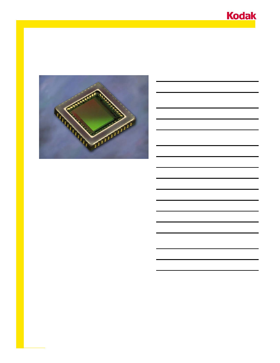
IMAGE SENSOR SOLUTIONS
5
IMAGE SENSOR SOLUTIONS
K A C - 1 3 1 0 R e v 4 ∑ w w w . k o d a k . c o m / g o / i m a g e r s 5 8 5 - 7 2 2 - 4 3 8 5 E m a i l : i m a g e r s @ k o d a k . c o m
SUMMARY SPECIFICATION
S U M M A R Y S P E C I F I C A T I O N
KODAK KAC-1310 SXGA CMOS
IMAGE SENSOR 1280 (H) x 1024 (V)
Features
∑ Ω" Color SXGA Advanced CMOS Image Sensor
∑ 1280 x 1024 active imaging pixels - progressive
scan
∑ Monochrome or Bayer (RGB or CMY) Color Filters
∑ 6.0µm pitch square pixels with microlenses
∑ Kodak patented pinned photodiode architecture;
high blue QE, low dark current, lag free
∑ High sensitivity, quantum efficiency, and charge
conversion efficiency
∑ True Correlated Double Sampling for low read
noise
∑ Low fixed pattern noise and wide dynamic range
∑ Antiblooming control and Continuous variable
speed rolling electronic shutter
∑ Single 3.3V power supply; Single master clock
∑ Digitally programmable via I
2
C-compatible interface
∑ Pixel addressability to support `Window of Interest'
windowing, resolution, and sub-sampling
∑ External sync signal for use with strobe flash
∑ On-chip 20x programmable gain for white balance
and exposure gain
∑ 10-bit, pipelined algorithmic RSD ADC
∑ 15 fps full SXGA at 20MHz Master Clock Rate
∑ 48 pin CLCC package
∑ Dark reference pixels with automatic Frame Rate
Dark Clamp
∑ Encoded Sync data stream
∑ Column offset correction circuitry
Parameter Value
Total Number of Pixels
1296 (H) x 1046 (V)
Number of Effective
Pixels
1288 (H) x 1032 (V)
Number of Active Pixels
1280 (H) x 1024 (V)
Pixel Size
6.0 µm (H) x 6.0 µm (V)
Imager Size
7.68 mm (H) x 6.14mm (V)
(~1/2")
Chip Size
14.22 mm (H) x 14.22 mm (V)
Optical Fill-Factor
40% mono / 64% color
Aspect Ratio
5:4
Saturation Signal
40,000 electrons
Quantum Efficiency
46% peak CMY
Responsivity
1.2 V/Lux-sec peak CMY
Total Dark Noise
70 e- rms
Dark Current
6250 e-/pixel/sec
Dark Current Doubling
Temperature
9
o
C
Dynamic Range
>54dB
Blooming Suppression
200x