
IMAGE SENSOR SOLUTIONS
D E V I C E
P E R F O R M A N C E
S P E C I F I C A T I O N
KODAK KAI-1010
KODAK KAI-1010M
KODAK KAI-1011CM
Image Sensor
1008 (H) x 1018 (V)
Interline Transfer
Progressive Scan CCD
October 28, 2002
Revision 8
K A I - 1 0 1 0 / 1 0 1 1 R e v 8 ∑ w w w . k o d a k . c o m / g o / i m a g e r s 5 8 5 - 7 2 2 - 4 3 8 5 i m a g e r s @ k o d a k . c o m

IMAGE SENSOR SOLUTIONS
Table of Contents
Features ..........................................................................................................................................................4
Features ..........................................................................................................................................................4
Description.....................................................................................................................................................5
Architecture....................................................................................................................................................5
Image Acquisition..........................................................................................................................................5
Charge Transport ...........................................................................................................................................6
Output Structure.............................................................................................................................................7
Electronic Shutter...........................................................................................................................................8
Color Filter Array (optional, for KAI-1011CM only) ...................................................................................8
Packaging Configuration ...............................................................................................................................9
Pin Description.............................................................................................................................................10
Absolute Maximum Range ..........................................................................................................................12
DC Operating Conditions ............................................................................................................................13
AC Clock Level Conditions.........................................................................................................................14
AC Timing Requirements for 20 MHz Operation .......................................................................................15
Frame Timing - Single Register Readout ..........................................................................................16
Line Timing - Single Register Readout .............................................................................................17
Pixel Timing - Single Register Readout ............................................................................................18
Electronic Shutter Timing - Single Register Readout........................................................................19
2
Line Timing - Dual Register Readout................................................................................................21
Frame Timing - Dual Register Readout.............................................................................................20
Pixel Timing - Dual Register Readout...............................................................................................22
Fast Dump Timing ≠ Removing Four Lines ......................................................................................23
Binning ≠ Two to One Line Binning .................................................................................................24
Timing ≠ Sample Video Waveform ...................................................................................................25
Image Specifications....................................................................................................................................26
Electro-Optical for KAI-1011CM......................................................................................................26
Electro-Optical for KAI-1010M ........................................................................................................28
CCD ...................................................................................................................................................31
Output Amplifier @ V
DD
= 15V, V
SS
= 0.0V ....................................................................................31
General...............................................................................................................................................32
Defect Classification....................................................................................................................................34
Climatic Requirements.................................................................................................................................35
Quality Assurance and Reliability ...............................................................................................................35
Ordering Information ...................................................................................................................................36
K A I - 1 0 1 0 / 1 0 1 1 R e v 8 ∑ w w w . k o d a k . c o m / g o / i m a g e r s 5 8 5 - 7 2 2 - 4 3 8 5 i m a g e r s @ k o d a k . c o m

IMAGE SENSOR SOLUTIONS
Figures
Figure 1 Functional Block Diagram ..............................................................................................................4
Figure 2 KAI-1011CM ..................................................................................................................................5
Figure 3 True 2 Phase CCD Cross Section....................................................................................................6
Figure 4 Output Structure ..............................................................................................................................7
Figure 5 CFA Pattern .....................................................................................................................................8
Figure 6 Device Drawing - Die Placement ....................................................................................................9
Figure 7 Pinout Diagram Top View.............................................................................................................11
Figure 8 Recommended Output Structure Load Diagram ...........................................................................13
Figure 9 Frame Timing - Single Register Readout......................................................................................16
Figure 10 Line Timing - Single Register Output .........................................................................................17
Figure 11 Pixel Timing Diagram - Single Register Readout.......................................................................18
Figure 12 Electronic Shutter Timing Diagram - Single Register Readout ..................................................19
Figure 13 Frame Timing - Dual Register Readout ......................................................................................20
Figure 14 Line Timing - Dual Register Output ...........................................................................................21
Figure 15 Pixel Timing Diagram - Dual Register Readout .........................................................................22
Figure 16 Fast Dump Timing - Removing Four Lines ................................................................................23
Figure 17 Binning - 2 to 1 Line Binning......................................................................................................24
Figure 18 Sample Video Waveform at 5MHz .............................................................................................25
Figure 19 Nominal KAI 1011CM Spectral Response .................................................................................27
Figure 20 Nominal KAI-1010M Spectral Response....................................................................................28
Figure 21 Angular Dependence of Quantum Efficiency .............................................................................29
Figure 22 Frame Rate versus Horizontal Clock Frequency.........................................................................30
Figure 23 Typical KAI-1010M Photoresponse............................................................................................32
Figure 24 Example of Vsat versus Vsub......................................................................................................33
Tables
Table 1 Package Pin Assignments ...............................................................................................................10
Table 2 Absolute Maximum Ranges............................................................................................................12
Table 3 DC Operating Conditions ...............................................................................................................13
Table 4 AC Clock Level Conditions............................................................................................................14
Table 5 AC Timing Requirements for 20 MHz Operation ..........................................................................15
Table 6 Electro-Optical Image Specifications KAI-1011CM .....................................................................26
Table 7 Electro-Optical Image Specifications KAI-1010M ........................................................................28
Table 8 CCD Image Specifications..............................................................................................................31
Table 9 Output Amplifier Image Specifications..........................................................................................31
Table 10 General Image Specifications .......................................................................................................32
Table 11 Climatic Requirements .................................................................................................................35
K A I - 1 0 1 0 / 1 0 1 1 R e v 8 ∑ w w w . k o d a k . c o m / g o / i m a g e r s 5 8 5 - 7 2 2 - 4 3 8 5 i m a g e r s @ k o d a k . c o m
3

IMAGE SENSOR SOLUTIONS
4
Features
∑ Front Illuminated Interline Architecture
∑ 1008 (H) x 1018 (V) Photosensitive Pixels
∑ 9.0µm(H) x 9.0µm(V) Pixel Size
∑ 9.1 mm(H) x 9.2 mm(V) Photosensitive Area
∑ Progressive Scan (Noninterlaced)
∑ Electronic Shutter
∑ Integral RGB Color Filter Array (optional)
∑ Advanced 2 Phase Buried Channel CCD
Processing
∑ On-Chip Dark Reference Pixels
∑ Low Dark Current
∑ Patented High Sensitivity Output Structure
∑ Dual Output Shift Registers
∑ Antiblooming Protection
∑ Negligible Lag
∑ Low Smear (0.01% with microlens)
4 dark lines at bottom of image
2 dark lines at top of image
6 da
r
k
c
o
lu
m
n
s
1
0
d
a
rk
co
l
u
mn
s
KAI-1010
Active Image Area:
1008 (H) x 1018 (V)
9.0 x9.0
µm
2
pixels
Horizontal Register A
6 dummies
2 dummies
V1
V2
Horizontal Register B
V1
V2
VOUTA
VOUTB
H1A
H2
H1B
VDD
VDD
VSS/OG
VSS/OG
VRD
R
WELL
VSUB
Figure 1 Functional Block Diagram
K A I - 1 0 1 0 / 1 0 1 1 R e v 8 ∑ w w w . k o d a k . c o m / g o / i m a g e r s 5 8 5 - 7 2 2 - 4 3 8 5 i m a g e r s @ k o d a k . c o m
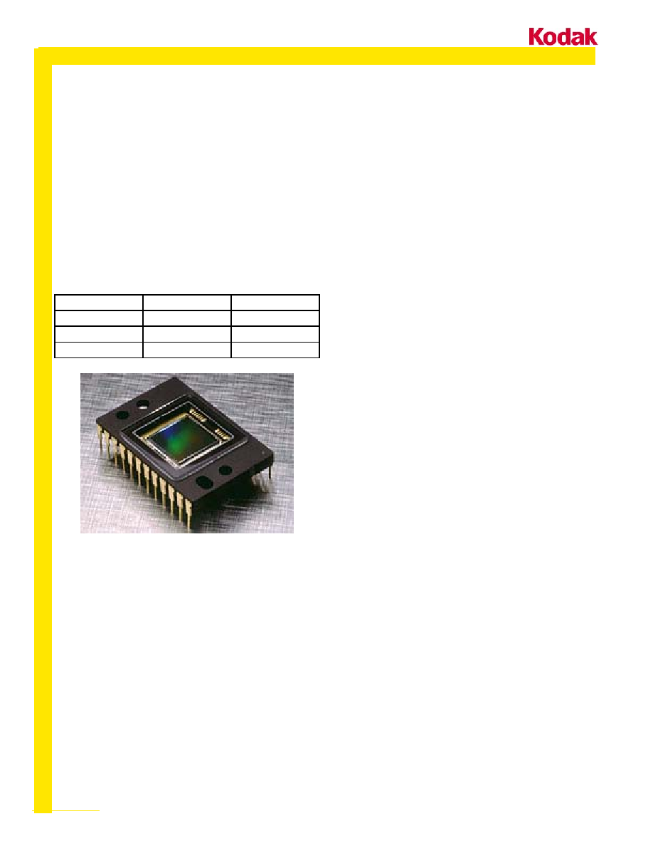
IMAGE SENSOR SOLUTIONS
5
Description
The KAI-1010 series is a high resolution charge coupled
device (CCD) image sensor whose noninterlaced
architecture makes it ideally suited for video, electronic
still and motion/still camera applications. The device is
built using an advanced true two-phase, double-
polysilicon, NMOS CCD technology. The p+npn-
photodetector elements eliminate image lag and reduce
image smear while providing antiblooming protection and
electronic-exposure control. The total chip size is 10.15
(H) mm x 10.00 (V) mm. The KAI-1010 comes in
monochrome and color versions, both with microlens for
sensitivity improvement.
Device Color Microlens
KAI-1010 No
No
KAI-1010M No
Yes
KAI-1011CM Yes
Yes
Figure 2 KAI-1011CM
Architecture
The KAI-1010 consists of 1024 x 1024 photodiodes, 1024
vertical (parallel) CCD shift registers (VCCDs), and dual
1032 pixel horizontal (serial) CCD shift registers
(HCCDs) with independent output structures. The device
can be operated in either single or dual line mode. The
advanced, progressive-scan architecture of the device
allows the entire image area to be read out in a single scan.
The active pixels are arranged in a 1008 (H) x 1018 (V)
array with an additional 16 columns and 6 rows of light-
shielded dark reference pixels.
Image Acquisition
An electronic representation of an image is formed when
incident photons falling on the sensor plane create
electron-hole pairs within the individual silicon
photodiodes. These photoelectrons are collected locally by
the formation of potential wells at each photosite. Below
photodiode saturation, the number of photoelectrons
collected at each pixel is linearly dependent on light level
and exposure time and non-linearly dependent on
wavelength. When the photodiode's charge capacity is
reached, excess electrons are discharged into the substrate
to prevent blooming.
K A I - 1 0 1 0 / 1 0 1 1 R e v 8 ∑ w w w . k o d a k . c o m / g o / i m a g e r s 5 8 5 - 7 2 2 - 4 3 8 5 i m a g e r s @ k o d a k . c o m