 | –≠–ª–µ–∫—Ç—Ä–æ–Ω–Ω—ã–π –∫–æ–º–ø–æ–Ω–µ–Ω—Ç: KLI-4104 | –°–∫–∞—á–∞—Ç—å:  PDF PDF  ZIP ZIP |

K L I - 4 1 0 4 - 4
w w w . k o d a k . c o m / g o / i m a g e r s E m a i l : i m a g e r s @ k o d a k . c o m 5 8 5 - 7 2 2 - 4 3 8 5
IMAGE SENSOR SOLUTIONS
1
D E V I C E
P E R F O R M A N C E
S P E C I F I C A T I O N
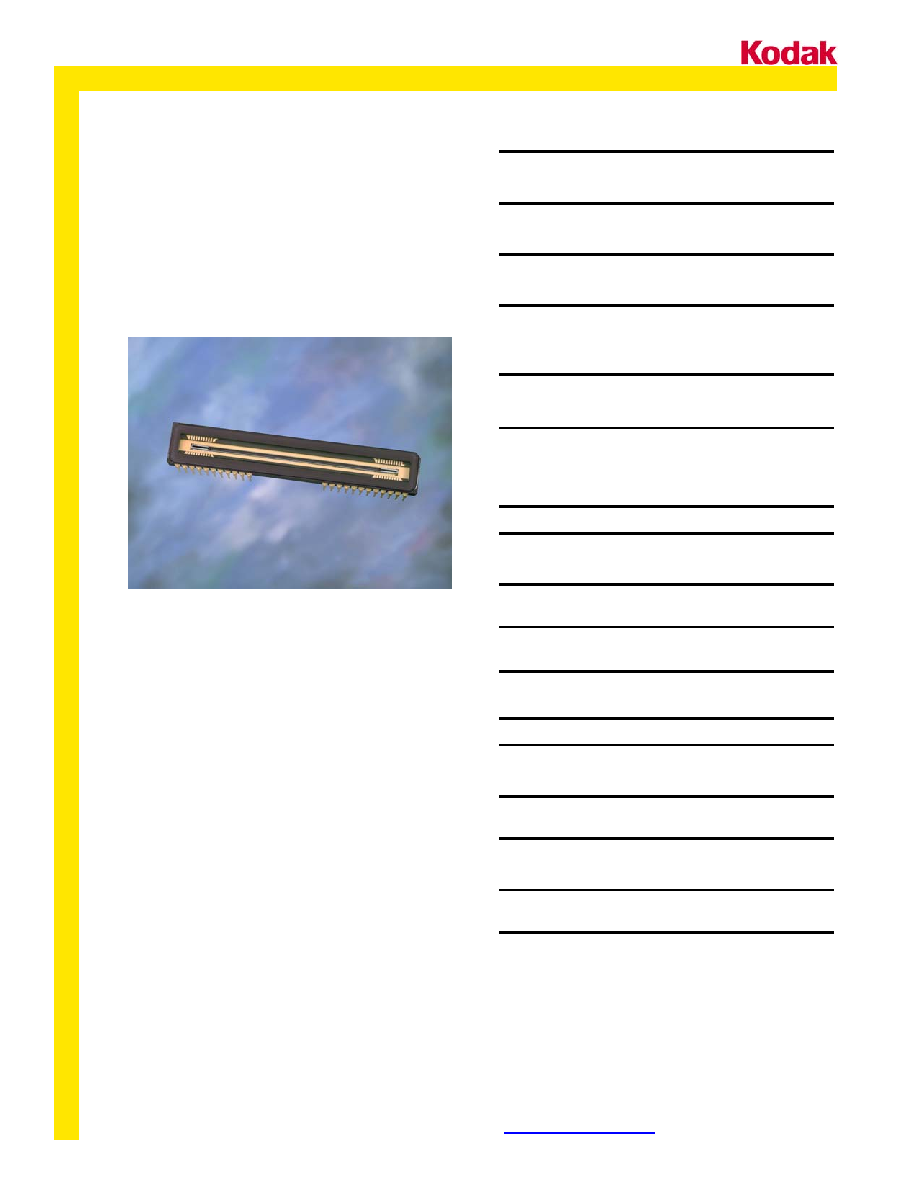
KODAK KLI-4104
Image Sensor
High-Resolution Quadri-Linear
Array 3 X 4080 Chroma, 10
µ
m
Square Pixels
and
Array 1 X 8160 Luma, 5
µ
m
Square
Pixels
October 27, 2003
Revision 4.0

K L I - 4 1 0 4 - 4
w w w . k o d a k . c o m / g o / i m a g e r s E m a i l : i m a g e r s @ k o d a k . c o m 5 8 5 - 7 2 2 - 4 3 8 5
IMAGE SENSOR SOLUTIONS
2
TABLE OF CONTENTS
TABLE OF FIGURES ............................................. 2
SUMMARY SPECIFICATIONS .............................. 3
PIN DESCRIPTION - KLI-4104 ............................. 4
SINGLE CHANNEL SCHEMATIC .......................... 5
GENERAL DESCRIPTION..................................... 6
IMAGE SPECIFICATIONS ..................................... 9
Chroma Channels................................................... 9
Luma Channel ...................................................... 10
IMAGE SPECIFICATION NOTES........................ 10
DEFECTIVE PIXEL
CLASSIFICATION ................................................ 12
COLOR FILTER RESPONSE AND
DESCRIPTION ..................................................... 13
Filter Variation Parameters................................... 14
ABSOLUTE MAXIMUM RATINGS ....................... 15
DC Bias Operating Conditions.............................. 17
Ac Electrical Characteristics ≠ AC Timing ............ 18
Electrical Characteristics AC ................................ 19
CLOCK LEVEL CONDITIONS FOR
OPERATION......................................................... 19
Transfer Timing Edge Alignment .......................... 21
Pixel Timing Detail................................................ 21
Pixel Timing Edge Alignment................................ 22
Clock Line Capacitance........................................ 23
TIMING DIAGRAM ............................................... 24
KLI-4104 FUNCTIONAL
DESCRIPTION ..................................................... 26
Chroma Imaging ................................................... 26
Luma Imaging ....................................................... 26
Charge Transport and Sensing ............................ 26
TYPICAL PERFORMANCE.................................. 27
STORAGE AND HANDLING................................ 29
Environmental Conditions..................................... 29
Handling Conditions ............................................. 29
ESD ...................................................................... 29
Soldering recommendations................................. 29
Cover glass care and cleanliness......................... 29
Environmental Exposure ...................................... 30
PACKAGE CONFIGURATION ............................. 31
QUALITY ASSURANCE AND RELIABILITY........ 35
REVISION CHANGES.......................................... 36
ORDERING INFORMATION ................................ 37
TABLE OF FIGURES
Figure 1 - Device Schematic .................................................5
Figure 2 ≠ Block Diagram......................................................6
Figure 3 ≠ Channel Alignment Diagram ................................7
Figure 4 ≠ Pixel Clock Video Output Table ...........................8
Figure 5 ≠ Defect Pixel Classification..................................12
Figure 6 ≠ Typical Responsivity ..........................................14
Figure 7 ≠ Device Input Protection Circuit...........................16
Figure 8 ≠ Typical Output Bias/Buffer Circuit ......................17
Figure 9 - Transfer Timing Edge Alignment ........................21
Figure 10 - Pixel Timing Detail ............................................21
Figure 11 ≠ H1 and H2 Edge Alignment..............................22
Figure 12 ≠ Line Timing Diagram ........................................24
Figure 13 ≠ Transfer Timing Diagram .................................24
Figure 14 ≠ Output Timing Diagram ....................................25
Figure 15 ≠ Typical Response Non-Linearity, luma ............27
Figure 16 ≠ Typical Response Non-Linearity, blue .............27
Figure 17 ≠ Typical CTE performance vs. H Clock Levels..28
Figure 18 ≠ Typical fixed charge loss vs OG at 30Mhz.......28
Figure 19 ≠ Package Configuration.....................................34
K L I - 4 1 0 4 - 4
w w w . k o d a k . c o m / g o / i m a g e r s E m a i l : i m a g e r s @ k o d a k . c o m 5 8 5 - 7 2 2 - 4 3 8 5
IMAGE SENSOR SOLUTIONS
3
SUMMARY SPECIFICATIONS
Description
The KODAK KLI-4104 Image Sensor is a
multi-spectral, linear solid-state image
sensor for color scanning applications
where fast high resolution is required. The
imager consists of three parallel linear
photodiode arrays, each with 4080 active
photosites for the output of R, G, and B
signals. The sensor contains a fourth
channel for luminance information. This
array has 8160 pixels segmented to
transfer out data through one of four
luminance outputs. This device offers high
sensitivity, high data rates, low noise and
negligible lag. Individual electronic
exposure control for each of the chroma
channels is provided, allowing the KLI-
4104 sensor to be used under a variety of
illumination conditions.
REVISION NO.: 4.0A
EFFECTIVE DATE: October XX, 2003
Parameter
Typical Value
Total Number of Pixels
3x4134 chroma,
1x8292 luma
Number of Effective
Pixels
3x4128 chroma,
1x8276 luma
Number of Active
Pixels
3x4080 chroma,
1x8160 luma
Pixel Size
10
µ
m (H) x 10
µ
m (V)
chroma,
5
µ
m (H) x 5
µ
m (V) luma
Pixel Pitch
10
µ
m chroma,
5
µ
m luma
Inter-Array Spacing, G
to R, R to B
B to L
90
µ
m (9 lines effective)
122.5
µ
m
(12.25 lines effective)
Chip Size
50.5 mm (H) x 1.1 mm (V)
Saturation Signal
132,000 electrons chroma,
100,000 electrons luma
Quantum Efficiency
62%(B), 62%(G), 80%(R),
85%(L)
Output Sensitivity
Chroma -14
µ
V/electron
Luma -11
µ
V/electron
Responsivity (R/G/B/L)
17(B), 20(G), 32(R),
27(L) V/
µ
J/cm2
Total Read Noise
120 electrons
Dark Current
Chroma 0.007 pA/pixel
Luma 0.0008 pA/pixel
Dark Current Doubling
Temperature
9∫C
Dynamic Range
@ 30 MHz Data Rate
60 dB (chroma)
60 dB (luma)
Photoresponse
Non-uniformity
5% Peak-Peak
Charge Transfer
Efficiency
0.99999/Transfer
KODAK KLI-4104
Image Sensor
Quadri-linear
CCD

K L I - 4 1 0 4 - 4
w w w . k o d a k . c o m / g o / i m a g e r s E m a i l : i m a g e r s @ k o d a k . c o m 5 8 5 - 7 2 2 - 4 3 8 5
IMAGE SENSOR SOLUTIONS
4
PIN DESCRIPTION - KLI-4104
Symbol
Description, Chroma
Pin
TG1C
Transfer Gate 1 Clock, chroma
6
TG2C
Transfer Gate 2 Clock, chroma
7
H1CA, H1CB
Phase 1 CCD Clock, chroma
15, 11
H2CA, H2CB
Phase 2 CCD Clock, chroma
14, 10
PHIRC
Reset Clock, chroma
22
OGCLA
Output Gate, chroma and low-pixels luma
26
RDC
Reset Drain, chroma
13
IDC
Test Input - Input Diode, chroma
8
IGC
Test Input - Input Gate, chroma
9
VIDx
Output Video (R,G,B)
19, 17, 21
VDDC Amplifier
Supply
(chroma)
25
SUBx
Ground Reference (R,G,B)
18, 16, 20
LOGx Exposure
Control
(R,G,B)
4,5,3
Symbol
Description, Luma
Pin
TG1L
Transfer Gate 1 Bias, luma
37
TG2L
Transfer Gate 2 Clock, luma
36
H1LA, H1LB
Phase 1 CCD Clock, luma
32, 39
H2LA, H2LB
Phase 2 CCD Clock, luma
33, 38
PHIRLA,PHIRLB Reset Clock luma
28, 43
OGLB
Output Gate, high pixels luma
45
RDLA, RDLB
Reset Drain, (low-, high-pixels luma)
34, 46
VIDLAO
Output Video, luma low-pixels, odd channel
31
VIDLAE
Output Video, luma low-pixels, even channel
29
VIDLBE
Output Video, luma high-pixels, even channel
40
VIDLBO
Output Video, luma high-pixels, odd channel
42
VDDLA, VDDLB Amplifier Supply (low-, high-pixels luma)
27, 44
SUBLA, SUBLB Ground Reference (low-, high-pixels luma)
30, 41
Symbol
Description, Device
Pin
LS
Light Shield / Exposure Drain
2
SUB
Substrate / Ground
1, 23
N/C
No Connection (recommend these pins at
ground)
12, 24, 35
23
22
21
20
19
18
13
14
15
16
17
33
32
31
30
29
28
27
26
25
24
34
46
45
44
43
42
41
40
39
38
37
36
Pixel 1
1
2
3
4
5
6
7
8
9
10
11
12
N/C
N/C
35
TG1L
H2LB
OGLB
VDDLB
PHIRLB
VIDLBA
TG2L
H1LB
VIDLBO
RDLB
SUBLB
SUB(DA)
IGC
IDC
TG2C
TG1C
H2CB
LS
LOGB
LOGR
LOGG
H1CB
SUB (DA)
SUBG
VIDG
SUBR
VIDR
PHIRC
RDC
SUBB
VIDB
H2CA
H1CA
VDDC
OGCLA
H2LA
H1LA
VIDLAO
SUBLA
N/C
VDDLA
PHIRLA
RDLA
VIDLAE

K L I - 4 1 0 4 - 4
w w w . k o d a k . c o m / g o / i m a g e r s E m a i l : i m a g e r s @ k o d a k . c o m 5 8 5 - 7 2 2 - 4 3 8 5
IMAGE SENSOR SOLUTIONS
5
SINGLE CHANNEL SCHEMATIC
H1L
A
PH
I
R
L
A
H2L
A
c
e
lls
4 bl
an
k
c
e
lls
4 bl
an
k
48
D
a
rk
4
080
A
c
ti
ve
Pi
x
e
l
s
RD
L
A
VD
DLA
VI
D
L
AO
SU
BL
A
VI
DL
AE
H
1LB
PH
IR
L
B
OG
L
B
H2
LB
c
e
lls
4 b
l
an
k
TG
2
L
TG
1
L
ce
ll
s
4 b
l
ank
48
Dar
k
4
080
A
c
tive
P
i
x
e
ls
RD
L
B
VDD
L
B
VI
D
L
B
O
SU
B
L
B
VI
D
L
B
E
Pi
x
e
l 1
4 B
l
an
k
Ce
l
l
s
2 B
l
an
k
Ce
lls
40
80
A
c
t
i
v
e
P
i
x
e
l
s
24
D
a
r
k
24
T
e
s
t
*
TG2
C
IGC
IDC
H1
C
B
H2
C
B
PH
IR
C
VID
x
( R
,
G
,
B
)
SU
B
x
(R,
G
,
B
)
TG1
C
Chroma C
h
ann
e
l
S
c
h
e
matic (1
o
f
3
chan
ne
ls, not
dr
aw
n to
scale)
VD
DC
OGC
LA
RD
C
6 Op
en
Pi
xel
s
16 D
a
rk
2 Dar
k
Description o
f
24
Te
st
Pixels fo
r
Chroma C
h
an
ne
l
*
Lu
ma Ch
a
n
n
e
l Sc
h
e
matic,
(n
o
t
d
r
aw
n
to
sc
ale)
H1
CA
H2
CA
L
OGx
(R
,
G
,
B
)
LS
Figure 1 - Device Schematic

K L I - 4 1 0 4 - 4
w w w . k o d a k . c o m / g o / i m a g e r s E m a i l : i m a g e r s @ k o d a k . c o m 5 8 5 - 7 2 2 - 4 3 8 5
IMAGE SENSOR SOLUTIONS
6
GENERAL DESCRIPTION
The KLI-4104 is a high resolution, quadri-linear
array designed for high-speed color scanning
applications. Each device contains 3 rows of 4080
active photoelements, consisting of high
performance 'pinned diodes' for improved
sensitivity, lower noise and the elimination of lag.
Each row is selectively covered with a red, green
or blue integral filter stripe for unparalleled spectral
separation. The pixel height and pitch is 10 micron
and the center-to-center spacing between color
channels is 90 microns, giving an effective nine
line delay between adjacent channels during
imaging.
Each device also contains 1 row of 8160 active
photoelements. This channel has a monochrome
response. The pixel height and pitch is 5 micron
and the center-to-center spacing between this
luminance channel and the blue color channel is
122.5 microns, giving an effective 12 º line delay.
Readout of the pixel data for each color channel is
accomplished through the use of a single CCD
shift register allowing for a single output per
channel with no multiplexing artifacts. Twenty-four
light shielded photoelements are supplied at the
start of each channel to act as a dark reference.
After the 4080 active pixels, the trailing region
contains 24 pixels dedicated for test. Only the first
16 pixels in this trailing group are configured to be
dark reference pixels. The remaining pixels are
used for internal testing. See the block diagram in
Figure 2.
Readout of the pixel data for the luminance
channel is accomplished through the use of four
CCD shift registers in an odd/even and left/right
readout configuration. Forty-eight light shielded
photoelements are supplied at the beginning of
each output channel to act as its dark reference. In
other words, twenty-four dark reference pixels are
on the leading edge of each luma output, none
trailing. See the block diagram in Figure 2.
The devices are manufactured using NMOS,
buried channel processing and utilize dual layer
polysilicon and dual layer metal technologies.
The die size is 50.50 mm X 1.10 mm and is
housed in a custom 46-pin, 0.400" wide, dual in
line package.
Figure 2 ≠ Block Diagram
VIDB
VIDR
VIDG
24
Dark
4080 Active Color Pixels
16
Dark
2
Blank
24
Dark
(ea.)
8160 Active Luminance Pixels
24
Dark
(ea.)
4 Blank
(ea.)
2040 Higher order pixels - odd
4 Blank
(ea.)
4 Blank
Pin 1 Corner
Chroma Pixel 1
Luma Pixel 1 Centered on Chroma Pixel 1 Leading Edge
VIDLAO
VIDLAE
VIDLBE
VIDLBO
2040 Lower order pixels - odd
2040 Higher order pixels - even
2040 Lower oder pixels - even
2
Dark
6
Optical
Inject
48 Dark
Pixels
48 Dark
Pixels

K L I - 4 1 0 4 - 4
w w w . k o d a k . c o m / g o / i m a g e r s E m a i l : i m a g e r s @ k o d a k . c o m 5 8 5 - 7 2 2 - 4 3 8 5
IMAGE SENSOR SOLUTIONS
7
Figure 3 ≠ Channel Alignment Diagram
9 lines spacing (90um)
9 lines spacing (90um)
12.25 lines spacing (122.5um)
Blue
Channel
Red
Channel
Green
Channel
Luma
Channel
first active pixel
(luma pixel #1)
last active pixel
(luma pixel #8160)
(c
en
ter)
(
edg
e)
PIN 1

K L I - 4 1 0 4 - 4
w w w . k o d a k . c o m / g o / i m a g e r s E m a i l : i m a g e r s @ k o d a k . c o m 5 8 5 - 7 2 2 - 4 3 8 5
IMAGE SENSOR SOLUTIONS
8
Figure 4 ≠ Pixel Clock Video Output Table
Pixel Clock
Cycle
VIDR
VIDG
VIDB
VIDLAO
VIDLAE
VIDLBO
VIDBLE
1
Blank(1)
Blank(1)
Blank(1)
Blank(1)
Blank(1)
Blank(1)
Blank(1)
2
Blank(2)
Blank(2)
Blank(2)
Blank(2)
Blank(2)
Blank(2)
Blank(2)
3
Blank(3)
Blank(3)
Blank(3)
Blank(3)
Blank(3)
Blank(3)
Blank(3)
(4)
4
Blank(4)
Blank(4)
Blank(4)
Blank(4)
Blank(4)
Blank(4)
Blank(4)
5
Dark(1)
Dark(1)
Dark(1)
Dark(1)
Dark(1)
Dark(1)
Dark(1)
6
Dark(2)
Dark(2)
Dark(2)
Dark(2)
Dark(2)
Dark(2)
Dark(2)
7
Dark(3)
Dark(3)
Dark(3)
Dark(3)
Dark(3)
Dark(3)
Dark(3)
8
Dark(4)
Dark(4)
Dark(4)
Dark(4)
Dark(4)
Dark(4)
Dark(4)
9
Dark(5)
Dark(5)
Dark(5)
Dark(5)
Dark(5)
Dark(5)
Dark(5)
.
.
.
26
Dark(22)
Dark(22)
Dark(22)
Dark(22)
Dark(22)
Dark(22)
Dark(22)
27
Dark(23)
Dark(23)
Dark(23)
Dark(23)
Dark(23)
Dark(23)
Dark(23)
(24)
28
Dark(24)
Dark(24)
Dark(24)
Dark(24)
Dark(24)
Dark(24)
Dark(24)
29
Active(1)
Active(1)
Active(1)
Active(1)
Active(2)
Active(8159) Active(8160)
30
Active(2)
Active(2)
Active(2)
Active(3)
Active(4)
Active(8157) Active(8158)
31
Active(3)
Active(3)
Active(3)
Active(5)
Active(6)
Active(8155) Active(8156)
32
Active(4)
Active(4)
Active(4)
Active(7)
Active(8)
Active(8153) Active(8154)
.
.
.
.
.
.
.
.
.
.
.
.
.
.
.
.
.
.
.
.
.
.
.
.
2066
Active(2038)
Active(2038)
Active(2038)
Active(4075) Active(4076) Active(4085) Active(4086)
2067
Active(2039)
Active(2039)
Active(2039)
Active(4077) Active(4078) Active(4083) Active(4084)
2068
Active(2040)
Active(2040)
Active(2040)
Active(4079) Active(4080) Active(4081) Active(4082)
2069
Active(2041)
Active(2041)
Active(2041)
Active(1)
Active(2)
Active(8159) Active(8160)
2070
Active(2042)
Active(2042)
Active(2042)
Active(3)
Active(4)
Active(8157) Active(8158)
2080
Active(2043)
Active(2043)
Active(2043)
Active(5)
Active(6)
Active(8155) Active(8156)
.
.
.
.
.
.
.
.
.
.
.
.
.
.
.
.
.
.
.
.
.
.
.
.
4105
Active(4077)
Active(4077)
Active(4077)
Active(4073) Active(4074) Active(4087) Active(4088)
4106
Active(4078)
Active(4078)
Active(4078)
Active(4075) Active(4076) Active(4085) Active(4086)
4107
Active(4079)
Active(4079)
Active(4079)
Active(4077) Active(4078) Active(4083) Active(4084)
4108
Active(4080)
Active(4080)
Active(4080)
Active(4079) Active(4080) Active(4081) Active(4082)
4109
Dark(1)
Dark(1)
Dark(1)
Dark(1)
Dark(1)
Dark(1)
Dark(1)
4110
Dark(2)
Dark(2)
Dark(2)
Dark(2)
Dark(2)
Dark(2)
Dark(2)
.
.
.
.
.
.
.
.
.
.
.
.
.
.
.
.
.
.
.
.
.
.
.
.
4123
Dark(15)
Dark(15)
Dark(15)
Dark(15)
Dark(15)
Dark(15)
Dark(15)
4124
Dark(16)
Dark(16)
Dark(16)
Dark(16)
Dark(16)
Dark(16)
Dark(16)
4125
Open(1)
Open(1)
Open(1)
Dark(17)
Dark(17)
Dark(17)
Dark(17)
4126
Open(2)
Open(2)
Open(2)
Dark(18)
Dark(18)
Dark(18)
Dark(18)
4127
Open(3)
Open(3)
Open(3)
Dark(19)
Dark(19)
Dark(19)
Dark(19)
4128
Open(4)
Open(4)
Open(4)
Dark(20)
Dark(20)
Dark(20)
Dark(20)
4129
Open(5)
Open(5)
Open(5)
Dark(21)
Dark(21)
Dark(21)
Dark(21)
4130
Open(6)
Open(6)
Open(6)
Dark(22)
Dark(22)
Dark(22)
Dark(22)
4131
Dark(17)
Dark(17)
Dark(17)
Dark(23)
Dark(23)
Dark(23)
Dark(23)
(24)
4132
Dark(18)
Dark(18)
Dark(18)
Dark(24)
Dark(24)
Dark(24)
Dark(24)
Blanks
4133
Blank(1)
Blank(1)
Blank(1)
(2) chroma
4134
Blank(2)
Blank(2)
Blank(2)
NOTE: 2 lines of luma channels per every chroma channel
OVERCLOCK FOR SYMMETRY
L
e
a
d
i
n
g
B
l
a
n
k
s
L
e
a
d
i
n
g
D
A
R
K
p
i
x
e
l
s
Clock hold during luma transfer transition to minimize noise feedthru
T
E
S
T
g
r
o
u
p
L
a
g
g
i
n
g
D
A
R
K
p
i
x
e
l
s
A
C
T
I
V
E
p
i
x
e
l
s

K L I - 4 1 0 4 - 4
w w w . k o d a k . c o m / g o / i m a g e r s E m a i l : i m a g e r s @ k o d a k . c o m 5 8 5 - 7 2 2 - 4 3 8 5
IMAGE SENSOR SOLUTIONS
9
IMAGE SPECIFICATIONS
Specifications given under nominally
specified operating conditions for the given
mode of operation @ 25oC, fCLK =30 MHz,
AR cover glass, color filters where
applicable, and an active load as shown in
Figure 4, unless otherwise specified. See
notes on next page for further descriptions
.
Chroma Channels
Symbol Parameter
Min.
Nom.
Max.
Units
Notes or
Remarks
Sampling
Plan
Vsat
Saturation Output Voltage, chroma
1.5
1.7
- - -
Vp-p
1, 8, 9, 17
die
deltaVo/deltaNe Output Sensitivity, chroma
- - -
14
- - -
µV/e-
8, 9
design
Ne,sat
Saturation Signal Charge, chroma
- - -
121K
- - -
electrons
1, 8, 9
design
R
Responsivity , chroma
2, 8, 9
Blue (@ 460 nm)
- - -
17
- - - V/microJ/cm2
± 10 %
Ref. die
Green (@ 550 nm)
- - -
20
- - - V/microJ/cm2
± 10 %
Ref. die
Red (@ 650 nm)
- - -
32
- - - V/microJ/cm2
± 10 %
Ref. die
DR
Dynamic Range, chroma
- - -
60
- - -
dB
3
design
DSNU
Dark Signal Non-Uniformity,chroma
- - -
2
16
mV
die
A
DC
DC Gain, amplifier, chroma
- - -
0.74
- - -
- - -
design
Idark
Dark Current, chroma @ 40∫C
- - -
0.007
2
pA/pixel
14, 17
die
CTE
Charge Transfer Efficiency, chroma @
30MHz data rate
0.99999 0.999992
- - -
- - -
17
design
Charge Transfer Efficiency, chroma @
2MHz data rate
0.999995 0.999997
- - -
- - -
4, 17
die
L
Lag, chroma @ 30MHz data rate
- - -
1
- - -
%
15
design
Lag, chroma @ 2MHz data rate
- - -
.005
- - -
%
4, 15, 17
die
Vo,dc
DC Output Offset, chroma
- - -
8.6
- - -
8, 9
design
PRNU, Low
Photoresponse Non-Uniformity chroma
Low Frequency
- - -
4
15
% p-p
5, 17
die
PRNU, Med
Photoresponse Non-Uniformity, chroma
Medium Frequency
- - -
4
15
% p-p
6, 17
die
PRNU, High
Photoresponse Non-Uniformity, chroma
High Frequency
- - -
4
15
% p-p
7, 17
die
Smear
Smear, chroma @450nm
- - -
0.03
- - -
%
design
Smear, chroma @500nm
- - -
0.05
- - -
%
design
Smear, chroma @550nm
- - -
0.1
- - -
%
design
Smear, chroma @600nm
- - -
0.2
- - -
%
design
Smear, chroma @650nm
- - -
0.3
- - -
%
design
RNL
Response Non-linearity
- - -
3
- - -
%
16
design
Dark Def
Darkfield Defect, chroma brightpoint
- - -
- - -
0
Allowed
11,17
die
Bfld Def
Brightfield Defect, chroma dark or bright
- - -
- - -
3
Allowed
10, 12,17
die
Exp Def
Exposure Control Defects, chroma only
- - -
- - -
64
Allowed
10, 13, Figure 5
die

K L I - 4 1 0 4 - 4
w w w . k o d a k . c o m / g o / i m a g e r s E m a i l : i m a g e r s @ k o d a k . c o m 5 8 5 - 7 2 2 - 4 3 8 5
IMAGE SENSOR SOLUTIONS
10
Luma Channel
Symbol Parameter
Min. Nom.
Max.
Units
Notes or
Remarks
Sampling
Plan
Vsat
Saturation Output Voltage, luma
1.0
1.3
- - -
Vp-p
1, 8, 9, 17
die
deltaVo/deltaNe Output Sensitivity, luma
- - -
11.5
- - -
µV/e-
8, 9
design
Ne,sat
Saturation Signal Charge, luma
- - -
110K
- - -
electrons 8,
9 design
R
Responsivity , luma (550nm)
6.5
V/microJ/cm2 2, 8, 9 (± 10 %)
die
DR
Dynamic Range, luma
- - -
60
- - -
dB
3
design
DSNU
Dark Signal Non-Uniformity, luma
- - -
2
16
mV
die
A
DC
DC Gain, amplifier, luma
- - -
0.74
- - -
- - -
design
Idark
Dark Current, luma @40∫C
- - -
0.0008
0.02
pA/pixel
14, 17
die
CTE
Charge Transfer Efficiency, luma @ 30
MHz data rate per luma channel
0.99999
0.999997
- - -
- - -
17
design
Charge Transfer Efficiency, luma @ 2 MHz
data rate per luma channel
0.999995
0.999997
- - -
- - -
4, 17
die
L
Lag, luma @ 30 MHz data rate per luma
channel
- - -
1
- - -
%
15
die
Lag, luma @ 2 MHz data rate per luma
channel
- - -
0.3
- - -
%
4, 15, 17
die
Vo,dc
DC Output Offset, luma
- - -
8.6
- - -
Volts
8, 9
design
PRNU, Low
Photoresponse Non-Uniformity luma Low
Frequency
- - -
4
10
% p-p
5, 17
die
PRNU, Med
Photoresponse Non-Uniformity, luma
Medium Frequency
- - -
4
10
% p-p
6, 17
die
PRNU, High
Photoresponse Non-Uniformity, luma High
Frequency
- - -
4
10
% p-p
7, 17
die
Smear
Smear @ 550nm
- - -
0.12
- - -
%
design
RNL
Response Non-linearity
- - -
3.4
- - -
%
16
design
Dark Def
Darkfield Defect, luma brightpoint
- - -
- - -
0
Allowed
11, 17
die
Bfld Def
Brightfield Defect, luma dark or bright
- - -
- - -
6
Allowed
10, 17, 18
die
IMAGE SPECIFICATION NOTES:
1. Defined as the maximum output level achievable before linearity or PRNU performance is
degraded beyond specification
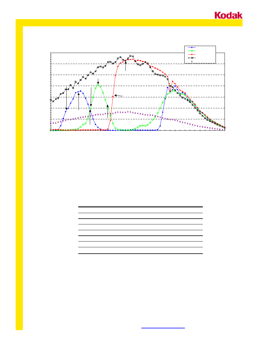
2. With color filter. Values specified at filter peaks. 50% bandwidth = ±30 nm. Color filter arrays
become transparent after 710 nm. It is recommended that a suitable IR cut filter be used to
maintain spectral balance and optimal MTF. See chart of typical responsivity later in this
document.
3. As measured at 30 MHz data rate. This device utilizes 2-phase clocking for cancellation of
driver displacement currents. Symmetry between PHI1 and PHI2 phases must be maintained
to minimize clock noise.
4. Measured per transfer. For a chroma line: (0.99999) * 8268 = 0.92065. For a luma line:
(0.99999) * 2092 = 0.97930.
5. Low frequency response is measured across the entire array with a 1000 pixel-moving
window and a 5 pixel median filter evaluated under a flat field illumination.
6. Medium frequency response is measured across the entire array with a 50 pixel-moving
window and a 5 pixel median filter evaluated under a flat field illumination.
7.
High frequency response non-uniformity represents individual pixel defects evaluated under a
flat field illumination. An individual pixel value may deviate above or below the average
response for the entire array. Zero individual
defects allowed per this specification.

K L I - 4 1 0 4 - 4
w w w . k o d a k . c o m / g o / i m a g e r s E m a i l : i m a g e r s @ k o d a k . c o m 5 8 5 - 7 2 2 - 4 3 8 5
IMAGE SENSOR SOLUTIONS
11
8. Increasing the current load (nominally 4.7 mA) to improve signal bandwidth will decrease
these parameters.
9. If resistive loads are used to set current, the amplifier gain will be reduced, thereby reducing
the output sensitivity and net responsivity.
10. Defective pixels will be separated by at least one non-defective pixel within and across
channels.
11. Pixels whose response is greater than the average response by the specified threshold,
(16mV). See line 1 in Figure 5.
12. Pixels whose response is greater or less than the average response by the specified
threshold, (±15%). See lines 2 and 3 in Figure 5.
13. Pixels whose response deviates from the average pixel response by the specified threshold,
(4.5mV), when operating in exposure control mode with an integration time that is 50% of the
line time. See lines 4 and 5 in figure below. If dark pattern correction is used with exposure
control, the dark pattern acquisition should be completed with exposure control actuated.
Dark current tends to suppress the magnitude of these defects as observed in typical
applications, hence line rate changes may affect perceived defect magnitude. Measured at
2MHz data rate.
14. Dark current doubles approximately every +9∞C.
15. Residual charge in the first field after transfer is used to determine lag measurement.
16. Nominal value is measured at an output of 1.5V signal level at 30MHz. Expect linearity to be
better than 10% over the entire range.
17. As measured at 2MHz data rate.
18. Pixels whose response is greater or less than the average response by the specified
threshold, (±10%). See lines 2 and 3 in Figure 5.

K L I - 4 1 0 4 - 4
w w w . k o d a k . c o m / g o / i m a g e r s E m a i l : i m a g e r s @ k o d a k . c o m 5 8 5 - 7 2 2 - 4 3 8 5
IMAGE SENSOR SOLUTIONS
12
DEFECTIVE PIXEL CLASSIFICATION
Exposure
Exposure
Signal Out
Signal Out
4
5
Linear
response of
a typical
pixel
3
2
1
Linear
response of
a typical
pixel
Figure 5 ≠ Defect Pixel Classification
Notes:
1 Dark Offset Error
2,3 Brightfield Defects; bright (2), or dark (3)
4,5 Exposure control mode defects, fast (4), or slow (5) pixels.

K L I - 4 1 0 4 - 4
w w w . k o d a k . c o m / g o / i m a g e r s E m a i l : i m a g e r s @ k o d a k . c o m 5 8 5 - 7 2 2 - 4 3 8 5
IMAGE SENSOR SOLUTIONS
13
COLOR FILTER RESPONSE AND DESCRIPTION
A filter set has been implemented for a series of
quad-linear image sensors optimized for high
sensitivity color scanning. Values for the various
nominal wavelength positions are shown below
with corresponding tolerances for responsivity and
wavelength as indicated for Color Image Sensors.
See Figure 1 for clarification of parameters.
Independent of filter type, a degree of variation in
the spectral response for the KLI-series quad-
linear image sensors can be expected from the
natural manufacturing tolerances of the process.
This variation is due to the combined variations in
filter properties (net density and filter peak
wavelength position) and the device properties
(sensitivity and film thickness variations).
Values for gauging filter performance are
determined from Figure 1. The center (or peak)
transmission wavelength is specified as
0, and
the 50% points are given as
1 and
2,
corresponding to the near and far wavelength
sides of the filter pass band.
For the red filter, only the near wavelength value is
presented. The red filter, as well as the blue and
green filters, exhibits a high level of transmission
beyond the 700nm (i.e., the filters become
transparent). The far wavelength edge is assumed
controlled by the system IR cut filter
characteristics.
K L I - 4 1 0 4 - 4
w w w . k o d a k . c o m / g o / i m a g e r s E m a i l : i m a g e r s @ k o d a k . c o m 5 8 5 - 7 2 2 - 4 3 8 5
IMAGE SENSOR SOLUTIONS
14
Figure 6 ≠ Typical Responsivity
Filter Variation Parameters
For Color Image Sensors
Wavelength
Filter Parameter
Wavelength
Responsivity Tolerance
Channel
(nm) Tolerance (nm)
(typical) 3
sigma (typical)
Green
0,g
540
± 12%
± 8
1,g
512 - ±
8
2,g
580 - ±
8
Blue
0,b
462
± 12%
± 8
1,b
415 - ±
8
2,b
508 - ±
8
Red
0,r
650 ±
12% -
1,r
602 - ±
8
KLI-4104 Image Sensor Typical Responsivity
0
5
10
15
20
25
30
35
350
450
550
650
750
850
950
1050
Wavelength (nm)
Re
s
pons
iv
ity
(V
/uJ
/
c
m
^2
)
Blue
Green
Red
no filter on chroma
Luma Channel
lambda 1,r
lambda 0,r
lambda 1,g
lambda 1,b
lambda 0,g
lambda 0,b
lambda 2,g
lambda 2,b

K L I - 4 1 0 4 - 4
w w w . k o d a k . c o m / g o / i m a g e r s E m a i l : i m a g e r s @ k o d a k . c o m 5 8 5 - 7 2 2 - 4 3 8 5
IMAGE SENSOR SOLUTIONS
15
ABSOLUTE MAXIMUM RATINGS
(SEE NOTE 8)
Parameter Symbol
Min.
Max.
Units
Notes
Gate Pin Voltages
VGate 0 16 V 1,
2
Pin-to-Pin Voltage
VPin-Pin 16 V 1,
3
Diode Pin Voltages
VDiode -0.5 16
V 1,
4
Output Bias Current
IDD -2 -8 mA 5
Output Load Capacitance
CVID,Load
10
pF 7
CCD Clocking Frequency
fclk 30
MHz
6
Notes:
1. Referenced to substrate voltage.
2. Includes
pins:
H1CA, H2CA, H2CA, H2CB, H1LA, H1LB, H2LA, H2LB, TG1C, TG2C, TG1L, TG2L, PHIRC,
PHIRLA, PHIRLB, OGCLA, OGLB, IGC, LOGR, and LOGG.
3. Voltage difference (either polarity) between any two pins.
4. Includes pins: VIDR, VIDG, VIDB, VIDLAO, VIDLAE, VIDLBO, VIDLBE, SUB(DA), SUBR, SUBG, SUBB,
SUBLA, SUBLB, RDC, RDLA, RDLB, VDDC, VDDLA, VDDLB, LS and IDC.
5. Care must be taken not to short output pins to ground during operation as this may cause permanent
damage to the output structures.
6. Charge transfer efficiency will degrade at frequencies higher than the maximum clocking frequency. VIDR,
VIDG, VIDB, VIDLAO, VIDLAE, VIDLBO, and VIDLBE load current values may need to be adjusted as well.
7. Exceeding the upper limit on output load capacitance will greatly reduce the output frequency response.
Thus, direct probing of the output pins with conventional oscilloscope probes is not recommended.
8. The absolute maximum ratings indicate the limits of this device beyond which damage may occur. The
Operating ratings indicate the conditions where the design should operate the device. Operating at or near
these ratings do not guarantee specific performance limits. Guaranteed specifications and test conditions
are contained in the Image Specifications section.

K L I - 4 1 0 4 - 4
w w w . k o d a k . c o m / g o / i m a g e r s E m a i l : i m a g e r s @ k o d a k . c o m 5 8 5 - 7 2 2 - 4 3 8 5
IMAGE SENSOR SOLUTIONS
16
Device Input ESD Protection Circuit (schematic)
CAUTION: To allow for maximum performance, this device was designed with limited
input protection; thus, it is sensitive to electrostatic induced damage. These devices
should be installed in accordance with strict ESD handling procedures!
Figure 7 ≠ Device Input Protection Circuit
To Device
Function
SUB
I/O Pin
V
t
- 20 V

K L I - 4 1 0 4 - 4
w w w . k o d a k . c o m / g o / i m a g e r s E m a i l : i m a g e r s @ k o d a k . c o m 5 8 5 - 7 2 2 - 4 3 8 5
IMAGE SENSOR SOLUTIONS
17
DC Bias Operating Conditions
Symbol Parameter
Min. Nom.
Max.
Units Notes
V
SUBR,
V
SUBG
V
SUBB
V
SUBLA
V
SUBLB
V
SUB(DA)
Substrate
----- 0 ----- V
V
TG1L
Accumulation Phase Bias, Luma
----- 0 0.5 V 2,
3
V
RDC
V
RDLA,
V
RDLAB,
Reset Drain Bias
10.5 11 11.5 V
2
V
VDD
V
VDD
V
VDD
V
VDD
Output Buffer Supply
14.5 15 15.5 V
2
I
IDDC
I
IDDLA
I
IDDLB
Output Bias Current/Channel
-2 -4.7 -8 mA 1,2
V
OGCLA,
V
OGLB
Output Gate Bias
0.5 0.7 0.9 V 2,
3
V
LS
Light Shield / Drain Bias
12 15 15.5 V 2
V
IGC
Test Pin - Input Gate
----- 0 ----- V 2,
3
V
IDC
Test Pin - Input Diode
12 15 15.5 V 2
Notes:
1. A current sink must be supplied for each output. Load capacitance should be minimized so as not to limit
bandwidth. Circuit below is just one solution.
2. Referenced to substrate voltage.
3. Do not exceed absolute maximum levels for diode pins voltage.
Typical Output Bias/Buffer Circuit
2N2369
or Similar*
R
X
=150
*
R
L
=750 Ohms *
0.1 microF
To Device
Output Pin: VIDn
(Minimize Path Length)
Buffered Output
VDD
Ohms
Figure 8 ≠ Typical Output Bias/Buffer Circuit
*Rx serves as the load bias for the on-chip amplifiers. Choose the values of Rx and RL to optimize for specific
operating frequency. Rx should not be less than 75 Ohms.

K L I - 4 1 0 4 - 4
w w w . k o d a k . c o m / g o / i m a g e r s E m a i l : i m a g e r s @ k o d a k . c o m 5 8 5 - 7 2 2 - 4 3 8 5
IMAGE SENSOR SOLUTIONS
18
Ac Electrical Characteristics ≠ AC Timing
Symbol Parameter
30MHz
Operation
1MHz
Operation
Max Units Remarks
1e = 1/fCLK
CCD Element Duration
0.033
1
--
µ
s
1e count
(note 3)
1L = tint, chroma Line/Integration Period
138.4
4156
--
µ
s
4156 counts
(notes 3, 4)
1L = tint, luma
Line/Integration Period
68.9
2087
--
µ
s
2087 counts
(notes 3, 4)
tpd, chroma
PD-CCD Transfer Period
0.533
16
--
µ
s
16e counts
(note 3, 5)
tpd, luma
PD-CCD Transfer Period
0.566
17
--
µ
s
17e counts
(note 3, 5)
ttg1
Transfer Gate 1 Clear
0.033
1
--
µ
s
1e count
(note 3)
ttg2
Transfer Gate 2 Clear
0.033
1
--
µ
s
1e count
(note 3)
tdr, chroma
Charge Drain Duration as
% of line time
-- --
90
%
Note
2
tdr, luma
Charge Drain Duration as % of
line time
-- --
90
%
Note
2
tcd
Clamp to H2 Delay
5
--
--
ns
Note 1
tsd
Sample to Reset Edge Delay
5
--
--
ns
Note 1
t
logrise
LOG rise time
0.066
2
--
µ
s
2e count
(note 3)
t
logfall
LOG fall time
0.066
2
--
µ
s
2e count
(note 3)
Notes:
1
Recommended delays for Correlated Double Sampling (CDS) of output.
2 Maximum value stated ensures proper linearity performance. Integration times shorter than 10% of the line
time increase device non-linearity.
3
Where noted as a multiple of CCD element durations, scale the appropriate times listed if the clock element
time changes.
4
This value represents the shortest line period. Integration time can be shorter than a line period with the use
of electronic exposure control or by extending the line period with horizontal overclocking.
5 If the application uses values less than those listed here expect degradation in lag and/or exposure control
performance, where appropriate.

K L I - 4 1 0 4 - 4
w w w . k o d a k . c o m / g o / i m a g e r s E m a i l : i m a g e r s @ k o d a k . c o m 5 8 5 - 7 2 2 - 4 3 8 5
IMAGE SENSOR SOLUTIONS
19
Electrical Characteristics AC
Clock Level Conditions For Operation
Symbol Parameter
Min.
2MHz
Operation
30MHz
Operation
Max. Units Notes
VH1x
H
,VH2x
H
CCD Readout Clocks High
6.25
6.5 7.25
9.0
V
3,
7
VH1x
L
,VH2x
L
CCD Readout Clocks Low
-0.1
0.0 0.0
0.1
V
1,
3
VTGx
H
Transfer Clocks High
6.25
6.5
7.25
9.0
V
4, 7
VTGx
L
Transfer Clocks Low
-0.1
0.0
0.0
0.1
V
1, 4
VPHIRx
H
Reset Clock High (Normal Mode)
6.25
6.5
7.25
9.0
V
5, 7
VPHIRx
L
Reset Clock Low
-0.1
0.0
0.0
0.1
V
1, 5
VLOGx
H
Exposure Clocks High
6.25
6.5
7.25
9.0
V
2, 6, 7
VLOGx
L
Exposure Clocks Low
-0.1
0.0
0.0
0.1
V
1, 2, 6
Notes:
1. Care should be taken to insure that low rail overshoot does not exceed -0.5 VDC. Exceeding this value may
result in non-photogenerated charged being injected into the video signal.
2. Connect pin to ground potential for applications where exposure control is not required.
3. where "x" can be "CA", "CB", "LA", or "LB".
4. where "x" can be "1C", "2C", or "2L". TG1L is a bias and is not clocked.
5. where "x" can be "C", "LA", or "LB".
6. where "x" can be "R", "G", or "B".
7. For high level clocks at 30MHz operation, use the values found in the "30MHz Operation" column. This value
represents the recommended setting for operation. Operating ranges for the high level clocks should be held
to a variation range of +/- 0.25. Clock levels below this range will result in loss of charge transfer efficiency
and other performance degradations.

K L I - 4 1 0 4 - 4
w w w . k o d a k . c o m / g o / i m a g e r s E m a i l : i m a g e r s @ k o d a k . c o m 5 8 5 - 7 2 2 - 4 3 8 5
IMAGE SENSOR SOLUTIONS
20
Clock Voltage Detail Characteristics (Note 1)
Description Symbol
Min
Nom
Max
Units
Notes
TG1x High-level variation
V1
HH
- 0.50 1 V High-level
coupling
TG2C High-level variation
V2
HL
- 0.28 1 V High-level
coupling
TG2C Low-level variation
V2
LH
- 0.46 1 V Low-level
coupling
TG1x Low-level variation
V1
LL
- 0.14 1 V Low-level
coupling
H1x High-level variation
H1
HH
- 0.30 1 V
H1x High-level variation
H1
HL
- 0.07 1 V
H1 Low-level variation
H1
LH
- 0.16 1 V
H1x Low-level variation
H1
LL
- 0.25 1 V
H2x High-level variation
H2
HH
- 0.40 1 V
H2x High-level variation
H2
HL
- 0.06 1 V
H2x Low-level variation
H2
LH
- 0.10 1 V
H2x Low-level variation
H2
LL
- 0.27 1 V
H1x ≠ H2x Cross-over
H1
CR1
40
50
60
%
Rising side of H1
H1x ≠ H2x Cross-over
H1
CR2
40
50
60
%
Falling side of H1
PHIRx High-level variation
RG
HH
- 0.19 1 V
PHIRx High-level variation
RG
HL
- 0.20 1 V
PHIRx Low-level variation
RG
LH
- 0.11 1 V
PHIRx Low-level variation
RG
LL
- 0.30 1 V
TG1x Rise Time
t
V1r
- 0.26 1 us
2
TG2C Rise Time
t
V2r
- 0.55 1 us
2
TG1x Fall Time
t
V1f
- 0.43 1 us
2
TG2C Fall Time
t
V2f
- 0.31 1 us
2
H1 Rise Time
t
H1r
- 9.0 10 ns
2
H2 Rise Time
t
H2r
- 6.9 10 ns
2
H1 Fall Time
t
H1f
- 5.8 10 ns
2
H2 Fall Time
t
H2f
- 5.4 10 ns
2
PHIRx Rise Time
t
RGr
- 2.0 4 ns
2
PHIRx Fall Time
t
RGf
- 2.2 4 ns
2
Notes:
1. H1, H2 clock frequency: 30MHz. The maximum and minimum values in this table are supplied for reference.
Testing against the device performance specifications is performed using the nominal values.
2. Longer times will degrade noise performance.

K L I - 4 1 0 4 - 4
w w w . k o d a k . c o m / g o / i m a g e r s E m a i l : i m a g e r s @ k o d a k . c o m 5 8 5 - 7 2 2 - 4 3 8 5
IMAGE SENSOR SOLUTIONS
21
Transfer Timing Edge Alignment
100%
90%
10%
0%
50%
V1
HH
V2
LH
V1
LL
t
w
t
r
t
f
t
overlap
V1
V2
V2
HL
Figure 9 - Transfer Timing Edge Alignment
Pixel Timing Detail
100%
90%
10%
0%
50%
RG
HL
RG
HH
RG
LL
RG
LH
t
RGw
t
RGr
t
RGf
Figure 10 - Pixel Timing Detail

K L I - 4 1 0 4 - 4
w w w . k o d a k . c o m / g o / i m a g e r s E m a i l : i m a g e r s @ k o d a k . c o m 5 8 5 - 7 2 2 - 4 3 8 5
IMAGE SENSOR SOLUTIONS
22
Pixel Timing Edge Alignment
100%
90%
10%
0%
50%
H1
H2
H1
CR1
H1
CR2
t
H1r
t
H2r
t
t
H1f
t
H2f
H1
LH
H1
LL
H2
LH
H2
LL
10%
0%
H1
HL
H1
HH
t
H2w
H2
HL
H2
HH
t
H1w
100%
90%
H2
H1
50%
H2
H1
Figure 11 ≠ H1 and H2 Edge Alignment

K L I - 4 1 0 4 - 4
w w w . k o d a k . c o m / g o / i m a g e r s E m a i l : i m a g e r s @ k o d a k . c o m 5 8 5 - 7 2 2 - 4 3 8 5
IMAGE SENSOR SOLUTIONS
23
Clock Line Capacitance
Chroma
Symbol Parameter
Min. Nom. Max Units Notes
C
H1CA
C
H1CB
Phase 1 Clock Capacitance
--
330
--
pF
1
C
H2CA
C
H2CB
Phase 2 Clock Capacitance
--
270
--
pF
1
C
TG1C
Transfer Gate 1 Capacitance
--
185
--
pF
C
TG2C
Transfer Gate 2 Capacitance
--
320
--
pF
C
LOGR
C
LOGG
C
LOGB
Exposure Gate Capacitance
--
33
--
pF
C
PHIRC
Reset Gate Capacitance
--
10
--
pF
Luma
Symbol Parameter
Min. Nom. Max Units Notes
C
H1LA
C
H1LB
Phase 1 Clock Capacitance
--
400
--
pF
C
H2LA
C
H2LB
Phase 2 Clock Capacitance
--
300
--
pF
C
TG2L
Transfer Gate 2 Capacitance
--
230
--
pF
C
PHIRLA
C
PHIRLB
Reset Gate Capacitance
--
6
--
pF
Notes:
1. The value listed is the effective value, or equal to Ω the total load capacitance per CCD phase. Since the
CCDs are driven from both ends of the sensor, the total load capacitance per horizontal drive function is
approximately twice the value listed. These values were calculated from design targets. These values do not
take into account the device package.

K L I - 4 1 0 4 - 4
w w w . k o d a k . c o m / g o / i m a g e r s E m a i l : i m a g e r s @ k o d a k . c o m 5 8 5 - 7 2 2 - 4 3 8 5
IMAGE SENSOR SOLUTIONS
24
TIMING DIAGRAM
TG2L
Line Timing, Luma
H1Lx
H2Lx
TG1C
LOGx
(R,G,B)
texp
H1Cx
H2Cx
TG2C
2040e
24e
4e
2040e
24e
4e
2040e
24e
4e
2040e
24e
4e
tint
24e
24e
2
e
24e
24e
tint
tdr
Line Timing, Chroma
2040e = Ω line
2040e = Ω line
2040e = Ω line
2040e = Ω line
Clock hold during TGxL transition to
minimize noise feedthru
4e
4e
19e
19e
2
e
2
e
2
e
2 overclock cycles to match chroma
and luma line timing
Figure 12 ≠ Line Timing Diagram
Luma Accumulation Gate-to-CCD Transfer Timing
1e
tpd
ttg2
First Dark Reference Pixel Data Valid
TG2L
H1Lx
H2Lx
1e
LOGx
(R,G,B)
ttg2
tdr
chroma
TG2C
H1Cx
H2Cx
tpd
ttg1
TG1C
Chroma Photodiode-to-CCD Transfer Timing
First Dark Reference Pixel Data Valid
Figure 13 ≠ Transfer Timing Diagram

K L I - 4 1 0 4 - 4
w w w . k o d a k . c o m / g o / i m a g e r s E m a i l : i m a g e r s @ k o d a k . c o m 5 8 5 - 7 2 2 - 4 3 8 5
IMAGE SENSOR SOLUTIONS
25
Figure 14 ≠ Output Timing Diagram
H2CCA, H2CB,
H2LA, H2LB
Output Timing
PHIRC, PHIRL
VIDLAO, VIDLAE,
VIDLBO, VIDLBE,
VIDR, VIDG,
VIDB
Clamp *
Sample *
tr
Vdark
Vsat
Vfeedthru
trst
tcd
tsd
* Required for Optional Off-Chip, Analog, Correlated Double Sampling (CDS) Signal Processing
1 Pixel

K L I - 4 1 0 4 - 4
w w w . k o d a k . c o m / g o / i m a g e r s E m a i l : i m a g e r s @ k o d a k . c o m 5 8 5 - 7 2 2 - 4 3 8 5
IMAGE SENSOR SOLUTIONS
26
KLI-4104
FUNCTIONAL DESCRIPTION
Chroma Imaging
During the integration period, an image is obtained
by gathering electrons generated by photons
incident upon the photodiodes. The charge
collected in the photodiode array is a linear
function of the local exposure. The charge is
stored in the photodiode itself and is isolated from
the CCD shift registers during the integration
period by the transfer gates TG1 and TG2, which
are held at barrier potentials. At the end of the
integration period, the CCD register clocking is
stopped with the H1 and H2 gates being held in a
'high' and 'low' state respectively. Next, the TG
gates are turned 'on' causing the charge to drain
from the photodiode into the TG1 storage region.
As TG1 is turned back 'off' charge is transferred
through TG2 and into the PHI1 storage region.
The TG2 gate is then turned 'off', isolating the shift
registers from the accumulation region once again.
Complementary clocking of the H1 and H2 phases
now resumes for readout of the current line of data
while the next line of data is integrated.
Luma Imaging
During the integration period, an image is obtained
by gathering electrons generated by photons
incident upon the photodiodes. The charge
collected in the photodiode array is a linear
function of the local exposure. The charge is
stored in the photodiode and an accumulation
region adjacent to the photodiode. This transfer
occurs with the bias applied to TG1L. The
accumulation storage region is isolated from the
CCD shift registers during the integration period by
the transfer gate TG2, which is held at barrier
potentials. At the end of the integration period, the
CCD register clocking is stopped with the H1Lx
and H2Lx gates being held in a 'high' and 'low'
state respectively.
Next, the TG2 gate is turned 'on' causing the
charge to drain from the accumulation region into
H1 storage region. The TG2 gate is then turned
'off', isolating the shift registers from the
accumulation region once again. Complementary
clocking of the H1 and H2 phases now resumes
for readout of the current line of data while the
next line of data is integrated.
Charge Transport and Sensing
In either the chroma or luma cases, readout of the
signal charge is accomplished by two-phase,
complementary clocking of the H1 and H2 gates,
(labeled H1Cx/H2Cx or H1Lx/H2Lx). The register
architecture has been designed for high speed
clocking with minimal transport and output signal
degradation, while still maintaining low (7.25Vp-p
min) clock swings for reduced power dissipation at
30MHz thereby, lowering clock noise and
simplifying the driver design. The data in all
registers is clocked simultaneously toward the
output structures. The signal is then transferred to
the output structures in a parallel format at the
falling edge of the H2 clocks. Re-settable floating
diffusions are used for the charge-to-voltage
conversion while source followers provide
buffering to external connections. The potential
change on the floating diffusion is dependent on
the amount of signal charge and is given by dVFD
= dQ/CFD. Prior to each pixel output, the floating
diffusion is returned to the RD level by the reset
clock, PHIR.

K L I - 4 1 0 4 - 4
w w w . k o d a k . c o m / g o / i m a g e r s E m a i l : i m a g e r s @ k o d a k . c o m 5 8 5 - 7 2 2 - 4 3 8 5
IMAGE SENSOR SOLUTIONS
27
Typical Performance
Figure 15 ≠ Typical Response Non-Linearity, luma
Figure 16 ≠ Typical Response Non-Linearity, blue
L32 W3-21102 NonLinearity @f=30Mhz, Luma Chan
-15
-10
-5
0
5
10
0
0.2
0.4
0.6
0.8
1
1.2
1.4
1.6
Signal (V)
LumaA
LumaB
L32 W3-21102 NonLinearity @f=30Mhz , Blue Chan
-10
-8
-6
-4
-2
0
2
4
6
8
10
0
0.5
1
1.5
2
2.5
Signal (V)

K L I - 4 1 0 4 - 4
w w w . k o d a k . c o m / g o / i m a g e r s E m a i l : i m a g e r s @ k o d a k . c o m 5 8 5 - 7 2 2 - 4 3 8 5
IMAGE SENSOR SOLUTIONS
28
Typical Performance, continued
Figure 17 ≠ Typical CTE performance vs. H Clock Levels
Figure 18 ≠ Typical fixed charge loss vs OG at 30Mhz.
L32-W3-21102 @ f=30Mhz
0.9999
0.99991
0.99992
0.99993
0.99994
0.99995
0.99996
0.99997
0.99998
0.99999
1
5.5
5.75
6
6.25
6.5
6.75
7
7.25
7.5
7.75
8
HSwing (V)
HC
T
E
LumaA
LumaB
Blue
L32 -W3 @ f=30Mhz
Hswing=6.5V
0
1
2
3
4
5
6
7
8
9
0
0.25
0.5
0.75
1
1.25
1.5
1.75
2
2.25
OG (V)
Fi
xe
d
Lo
ss(
%
)
LumaA
LumaB
Blue

K L I - 4 1 0 4 - 4
w w w . k o d a k . c o m / g o / i m a g e r s E m a i l : i m a g e r s @ k o d a k . c o m 5 8 5 - 7 2 2 - 4 3 8 5
IMAGE SENSOR SOLUTIONS
29
STORAGE AND HANDLING
Environmental Conditions
Description Symbol
Minimum
Maximum
Units
Notes
Humidity
RH 5 90
%
1
Storage Temperature
T
ST
-25 80
∞
C
2
Operating Temperature
T
OP
0 70
o
C 3
Guaranteed Temperature
of Performance
T
SP
25 40
∞
C
4
Notes:
1. T=25
∞
C. Excessive humidity will degrade MTTF.
2. Long-term storage toward the maximum temperature may accelerate color filter degradation.
3. Noise
performance
will
degrade at higher temperatures.
4. See section for Imaging Performance Specifications.
Handling Conditions
ESD
1. This device contains limited protection against Electrostatic Discharge (ESD). Devices should be
handled in accordance with strict ESD procedures for Class 0 devices (< 250V JESD22-A114-B
Human Body Model) or Class A (< 200V JESD22-A114-A Machine Model). Refer to Application
Note MTD/PS-0224, Electrostatic Discharge Control, for proper handling and grounding
procedures. This application note also contains recommendations for workplace modifications for
the minimization of electrostatic discharge.
2. Devices are shipped in static-safe containers and should only be handled at static-safe
workstations.
Note: Also see section on Quality Assurance and Reliability.
Soldering recommendations
1. The soldering iron tip temperature is to not exceed 370
∞
C. Failure to do so may alter device
performance and reliability.
2. Flow soldering method is not recommended. Solder dipping can cause damage to the glass and
harm the imaging capability of the device. Recommended method is by partial heating. Kodak
recommends the use of a grounded 30W soldering iron. Heat each pin for less than 2 seconds
duration.
3. For circuit board repair, or de-soldering an image sensor, do not use solder suction equipment. In
any instance, care should be given to minimize and eliminate electrostatic discharge.
Cover glass care and cleanliness

K L I - 4 1 0 4 - 4
w w w . k o d a k . c o m / g o / i m a g e r s E m a i l : i m a g e r s @ k o d a k . c o m 5 8 5 - 7 2 2 - 4 3 8 5
IMAGE SENSOR SOLUTIONS
30
1. Devices are shipped with the cover glass region covered with a protective tape. The tape should
be removed upon usage.
Note: Also see section on Quality Assurance and Reliability.
Environmental Exposure
1. Do not expose to strong sun light for long periods of time. The color filters may become
discolored. Long time exposures to a static high contrast scene should be avoided. The image
sensor may become discolored and localized changes in response may occur from color filter
aging.
2. Exposure to temperatures exceeding the absolute maximum levels should be avoided for storage
and operation. Color filter performance may be degraded. Failure to do so may alter device
performance and reliability.
3. Avoid sudden temperature changes.
4. Exposure to excessive humidity will affect device characteristics and should be avoided. Failure
to do so may alter device performance and reliability.
5. Avoid storage of the product in the presence of dust or corrosive agents or gases.
6. Long-term storage should be avoided. Deterioration of lead solderability may occur. It is advised
that the solderability of the device leads be re-inspected after an extended period of storage, over
one year.

K L I - 4 1 0 4 - 4
w w w . k o d a k . c o m / g o / i m a g e r s E m a i l : i m a g e r s @ k o d a k . c o m 5 8 5 - 7 2 2 - 4 3 8 5
IMAGE SENSOR SOLUTIONS
31
PACKAGE CONFIGURATION

K L I - 4 1 0 4 - 4
w w w . k o d a k . c o m / g o / i m a g e r s E m a i l : i m a g e r s @ k o d a k . c o m 5 8 5 - 7 2 2 - 4 3 8 5
IMAGE SENSOR SOLUTIONS
32

K L I - 4 1 0 4 - 4
w w w . k o d a k . c o m / g o / i m a g e r s E m a i l : i m a g e r s @ k o d a k . c o m 5 8 5 - 7 2 2 - 4 3 8 5
IMAGE SENSOR SOLUTIONS
33

K L I - 4 1 0 4 - 4
w w w . k o d a k . c o m / g o / i m a g e r s E m a i l : i m a g e r s @ k o d a k . c o m 5 8 5 - 7 2 2 - 4 3 8 5
IMAGE SENSOR SOLUTIONS
34
Figure 19 ≠ Package Configuration

K L I - 4 1 0 4 - 4
w w w . k o d a k . c o m / g o / i m a g e r s E m a i l : i m a g e r s @ k o d a k . c o m 5 8 5 - 7 2 2 - 4 3 8 5
IMAGE SENSOR SOLUTIONS
35
QUALITY ASSURANCE AND RELIABILITY
Quality Strategy: All image sensors will conform to the specifications stated in this document. This will
be accomplished through a combination of statistical process control and inspection at key points of the
production process. Typical specification limits are not guaranteed but provided as a design target. For
further information refer to ISS Application Note MTD/PS-0292, Quality and Reliability.
Replacement: All devices are warranted against failure in accordance with the terms of Terms of Sale.
This does not include failure due to mechanical and electrical causes defined as the liability of the
customer below.
Liability of the Supplier: A reject is defined as an image sensor that does not meet all of the
specifications in this document upon receipt by the customer.
Liability of the Customer: Damage from mechanical (scratches or breakage), electrostatic discharge
(ESD) damage, or other electrical misuse of the device beyond the stated absolute maximum ratings,
which occurred after receipt of the sensor by the customer, shall be the responsibility of the customer.
Cleanliness: Devices are shipped free of mobile contamination inside the package cavity. Immovable
particles and scratches that are within the imager pixel area and the corresponding cover glass region
directly above the pixel sites are also not allowed. The cover glass is highly susceptible to particles and
other contamination. Touching the cover glass must be avoided. See ISS Application Note MTD/PS-0237,
Cover Glass Cleaning for Image Sensors, for further information.
ESD Precautions: Devices are shipped in static-safe containers and should only be handled at static-
safe workstations. See ISS Application Note MTD/PS-0224, Electrostatic Discharge Control, for handling
recommendations.
Reliability: Information concerning the quality assurance and reliability testing procedures and results are
available from the Image Sensor Solutions and can be supplied upon request. For further information
refer to ISS Application Note MTD/PS-0292, Quality and Reliability.
Test Data Retention: Image sensors shall have an identifying number traceable to a test data file. Test
data shall be kept for a period of 2 years after date of delivery.
Mechanical: The device assembly drawing is provided as a reference. The device will conform to the
published package tolerances.

K L I - 4 1 0 4 - 4
w w w . k o d a k . c o m / g o / i m a g e r s E m a i l : i m a g e r s @ k o d a k . c o m 5 8 5 - 7 2 2 - 4 3 8 5
IMAGE SENSOR SOLUTIONS
36
REVISION CHANGES
Revision
Number
Description of Changes
A
Initial release of preliminary specification
B
Pixel counts corrected, detailed description on dark pixel
region, some typical parameters updated, filter wavelength
tolerance identified, pixel timing updated,
C
Assembly drawings updated to revision 2.
D
Capacitance values added, pin-out pin 29 correction,
Coverglass cleaning procedure document number change
E
Capacitance values updated.
1A
Initial release. 30MHz operation, clarity, typical performance
graphs, defined specification limits, drawing to rev.3.
1B
Dark Current clarification
2
OG bias changed to 0.7V
3.0
Updated exposure control features for the chroma only. Luma
channel does not have exposure control.
4.0
Performance values finalized per production characterization.
Correction to general part description on page 6.

K L I - 4 1 0 4 - 4
w w w . k o d a k . c o m / g o / i m a g e r s E m a i l : i m a g e r s @ k o d a k . c o m 5 8 5 - 7 2 2 - 4 3 8 5
IMAGE SENSOR SOLUTIONS
37
ORDERING INFORMATION
Please contact Image Sensor Solutions for available part numbers.
Address all inquiries and purchase orders to:
Image Sensor Solutions
Eastman Kodak Company
Rochester, New York 14650-2010
Phone: (585) 722-4385
Fax: (585) 477-4947
E-mail:
imagers@kodak.com
Kodak reserves the right to change any information contained herein without notice. All information
furnished by Kodak is believed to be accurate.
WARNING: LIFE SUPPORT APPLICATIONS POLICY
Kodak image sensors are not authorized for and should not be used within Life Support Systems without
the specific written consent of the Eastman Kodak Company. Product warranty is limited to replacement
of defective components and does not cover injury or property or other consequential damages.