Photocoupler
The K101 has one channel in a 4-pin mini-flat SMD package.
The K102 has two channels in a 8-pin mini-flat SMD package.
The K104 has four channels in a 16-pin mini-flat SMD package.
FEATURES
∑ Mini-Flat Package
∑ Collector-Emitter Voltage : Min.50V
∑ Current Transfer Ratio : Min.50% (at I
F
=5mA, V
CE
=5V)
∑ Electrical Isolation Voltage : AC3750V
rms
APPLICATIONS
∑ Programmable Logic Control
∑ Microcomputer
K101 ∑ K102 ∑ K104
These Photocouplers consist of a Gallium Arsenide Infrared Emitting
Diode and a Silicon NPN Phototransistor per a channel.
∑ Interface between two circuits of different potential
∑ Cordless Phone
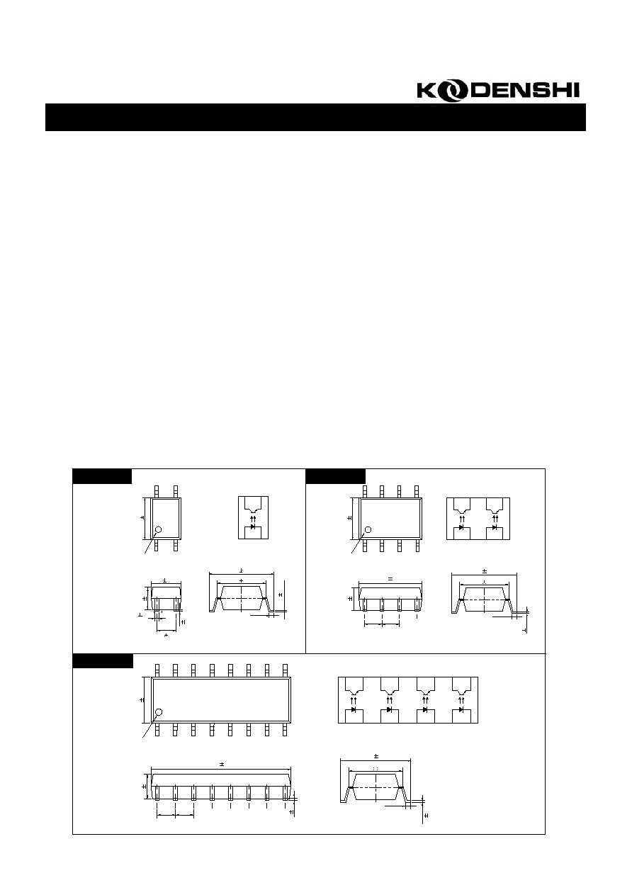
DIMENSION (Unit : mm)
K101
K102
K104
Orientation Mark
4
.
4
0
.
2
2.54 0.25
3.6 0.2
0.4 0.1
0
.
1
0
.
1
2
.
5
0
.
2
5.2 0.2
7.0 0.5
0.4Min.
0
.
1
5
0
.
0
5
1
2
4 3
4
.
4
0
.
2
2
.
5
0
.
2
8.7 0.2
8 6
5
7
2 3
4
1
Orientation Mark
0
.
1
5
0
.
0
5
0.4Min.
7.0 0.5
5.2 0.2
2.54 2.54
4
.
4
0
.
2
18.8 0.2
1
15 13
11 9
14
16 12 10
4
3
2 6
5 7
8
Orientation Mark
5.2 0.2
7.0 0.5
0.4Min.
2
.
5
0
.
2
0
.
1
0
.
1
2.54 2.54
1/3
0
.
1
5
0
.
0
5

Photocoupler
MAXIMUM RATINGS (Ta=25
)
*1. Input current with 100
µ
s pulse width, 1% duty cycle
*2. Measured at RH=40~60% for 1min
*3. 1/16 inch form case for 10sec
ELECTRO-OPTICAL CHARACTERISTICS
(Ta=25
, unless otherwise noted)
I
F
=10mA
V
R
=5V
V=0, f=1MHz
I
C
=0.5mA
I
E
=0.1mA
I
F
=0, V
CE
=24V
V
CE
=0, f=1MHz
I
F
=5mA, V
CE
=5V
I
F
=5mA, I
C
=1mA
V=0, f=1MHz
V
CE
=5V, R
L
=100
I
C
=2mA
*4. CTR=(I
C
/I
F
) X 100 (%)
Parameter
Symbol
Rating
Unit
Input
Forward Current
I
F
Reverse Voltage
V
R
Peak Forward Current
*1
I
FP
Power Dissipation
P
D
50
mA
5
V
1
A
70
mW
Output
Collector-Emitter Breakdown Voltage
BV
CEO
50
Emitter-Collector Breakdown Voltage
BV
ECO
6
Collector Current
I
C
50
V
V
mA
Collector Power Dissipation
P
C
150
mW
Input to Output Isolation Voltage
*2
V
iso
AC3750
V
rms
Storage Temperature T
stg
-55~+125
Operating Temperature T
opr
-30~+100
Total Power Dissipation
P
tot
200
mW
Collector Dark Current
Input-Output Isolation Resistance
Input-Output Capacitance
Capacitance
Current Transfer Ratio
*4
Collector-Emitter Saturation Voltage
Input
Output
Forward Voltage
Capacitance
Reverse Current
Collector-Emitter Breakdown Voltage
Emitter-Collector Breakdown Voltage
600
-
-
tr
-
R
IO
0.15
1
10
11
C
IO
V
V
nA
-
pF
%
V
pF
-
pF
Symbol
V
F
I
R
Max.
1.30
10
-
-
-
100
-
Unit.
-
-
0.4
-
-
3
- -
Typ.
1.15
V
K101 ∑ K102 ∑ K104
Parameter
Lead Soldering Temperature
*3
T
sol
260
-
Min.
-
-
50
6
-
30
50
3
-
-
-
10
-
tf
C
T
BV
CEO
CTR
V
CE(SAT)
BV
ECO
I
CEO
C
CE
RH=40~60%, V=500V
Coupled
Rise Time
Fall Time
Condition
2/3
Photocoupler
K101 ∑ K102 ∑ K104
3/3
Ambient Temperature T
a
( )
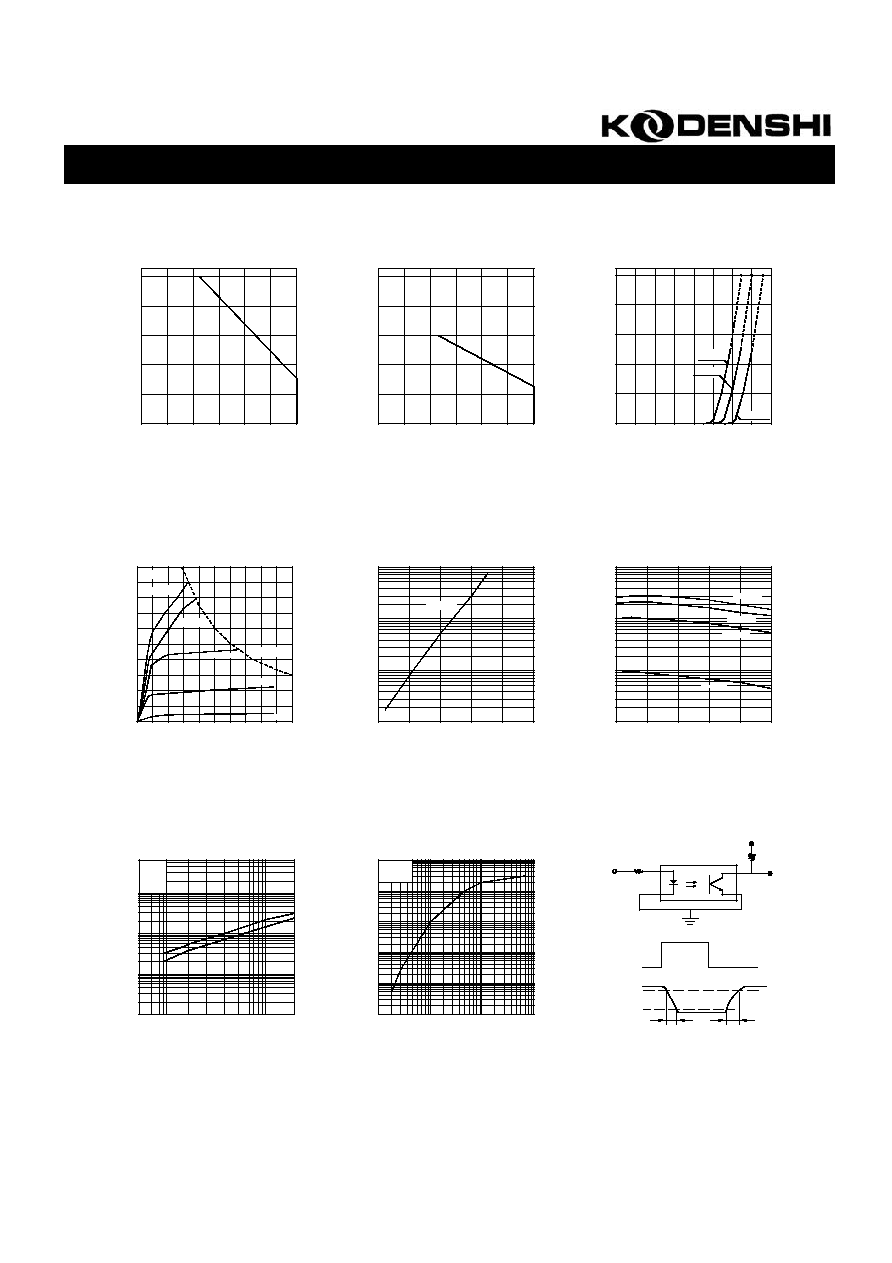
Forward Current vs.
Ambient Temperature
0
-20 0 20
F
o
r
w
a
r
d
C
u
r
r
e
n
t
I
F
(
m
A
)
10
20
40
30
50
Collector Current vs.
Forward Current
Forward Current I
F
(mA)
40 60 100
0.1 1
C
o
l
l
e
c
t
o
r
C
u
r
r
e
n
t
I
C
(
m
A
)
0.1
1
100
10
Collector-Emitter Voltage V
CE
(V)
Collector Current vs.
Collector-Emitter Voltage
0
2
4
6
C
o
l
l
e
c
t
o
r
C
u
r
r
e
n
t
I
C
(
m
A
)
8
10
80
D
a
r
k
C
u
r
r
e
n
t
I
C
E
O
(
)
Ambient Temperature T
a
( )
0
0.001
0.01
40
20
0.1
1
80
60 100
Dark Current vs.
Ambient Temperature
Collector Power Dissipation vs.
Ambient Temperature
C
o
l
l
e
c
t
o
r
P
o
w
e
r
D
i
s
s
i
p
a
t
i
o
n
P
C
(
m
W
)
-20
0
50
100
150
200
250
Ambient Temperature T
a
( )
20
0 60
40 100
80
100
0.001
0.01
10
10
20
30
40
C
o
l
l
e
c
t
o
r
C
u
r
r
e
n
t
I
C
(
m
A
)
0 40
20 80
60
Ambient Temperature T
a
( )
Collector Current vs.
Ambient Temperature
10
0
1
100
Output
Input
Test Circuit
V
IN
R
R
L
V
O
V
CC
Wave form
10%
90%
Switching Time Test Circuit
tr
tf
-20
T
a
=25
I
F
=30mA
I
F
=20mA
I
F
=10mA
I
F
=5mA
I
F
=1mA
P
C
(max.)
V
CE
=24V
I
F
=20mA
I
F
=10mA
I
F
=5mA
I
F
=1mA
T
a
=25
V
CE
=5V
Forward Voltage V
F
(V)
0.4
Forward Current vs.
Forward Voltage
F
o
r
w
a
r
d
C
u
r
r
e
n
t
I
F
(
m
A
)
20
0
60
40
100
80
1.6
T
a
=25
T
a
=70
0.8
T
a
=-55
1.2
Response Time vs.
Load Resistance
Load Resistance R
L
()
500
100
10
0.1
R
e
s
p
o
n
s
e
T
i
m
e
t
r
,
t
f
(
s
)
1
0.1
V
CE
=5V
I
C
=2mA
T
a
=25
tr
1.0
2.0
tf