Photocoupler
FEATURES
∑ Switching Time - Type 3
∑ Collector-Emitter Voltage : Min.35V
∑ Current Transfer Ratio : Typ.10% (at I
F
=
±
10mA, V
CE
=10V)
∑ Electrical Isolation Voltage : AC2500V
rms
∑ Without Base Connection - K3630
∑ With Base Connection - K3631
∑ UL Recognized File No. E107486
APPLICATIONS
∑ Interface between two circuits of different potential
∑ Telephone set & line interface
∑ I/O compatible with integrated circuits
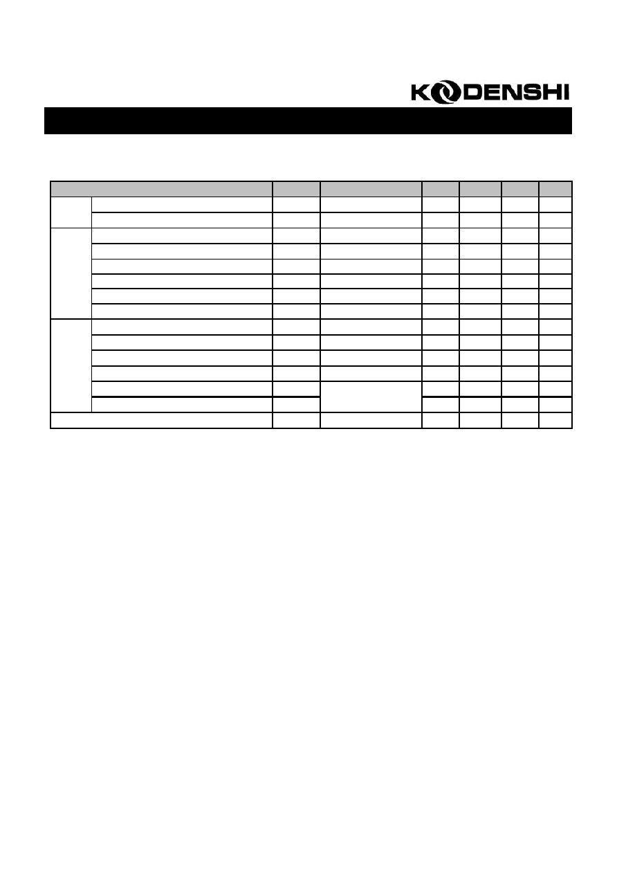
MAXIMUM RATINGS
(Ta=25
)
** Except for K3630
*1. Input current with 100
pulse width, 1% duty cycle
*2. Measured at RH=40~60% for 1min
*3. 1/16 inch form case for 10sec
∑ AC signal input
Emitter-Base Breakdown Voltage**
BV
EBO
6
K3630 ∑ K3631
These Photocouplers consist of two Gallium Arsenide Infrared Emitting
Diodes and a Silicon NPN Phototransistor in a 6-pin package.
260
Collector Power Dissipation
P
C
Lead Soldering Temperature
*3
T
sol
Operating Temperature T
opr
-30~+100
Storage Temperature T
stg
-55~+125
Input to Output Isolation Voltage
*2
V
iso
AC2500
V
rms
150
mW
V
V
V
V
Collector Current
I
C
50
mA
Emitter-Collector Breakdown Voltage
BV
ECO
6
Collector-Base Breakdown Voltage** BV
CBO
70
mA
A
Power Dissipation P
D
70 mW
Total Power Dissipation
Peak Forward Current
*1
I
FP
±
1
P
tot
200
Output
Collector-Emitter Breakdown Voltage
BV
CEO
35
Input
Forward Current I
F
±
60
Parameter
Symbol
Rating
Unit
mW
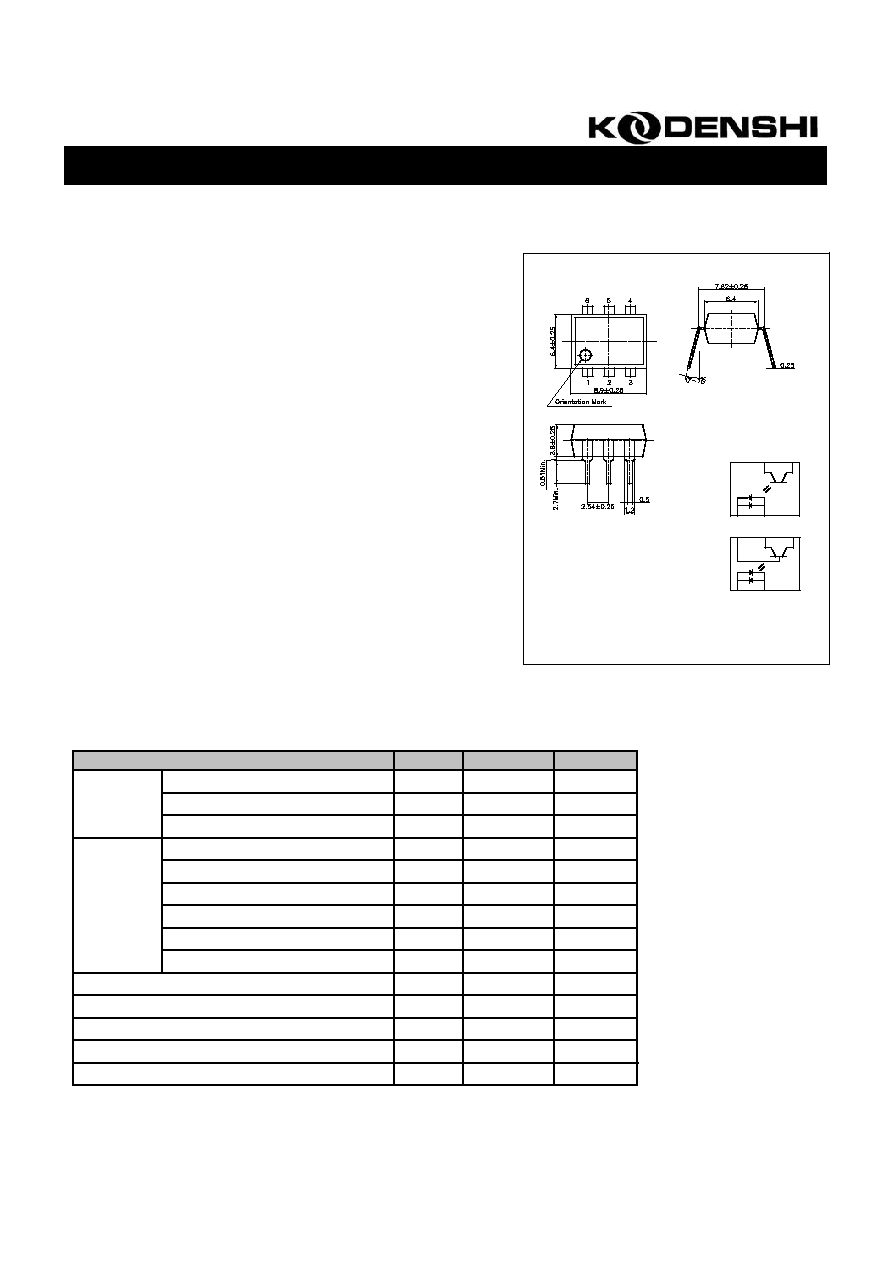
DIMENSION
(Unit : mm)
1/3
3
2
1
6
5
4
4
5
6
1
2
3
PIN NO. AND INTERNAL
CONNECTION DIAGRAM
K3630
K3631
Photocoupler
ELECTRO-OPTICAL CHARACTERISTICS
(Ta=25
, unless otherwise noted)
I
F
=10mA
V=0, f=1MHz
I
C
=1mA
I
E
=0.1mA
I
C
=0.1mA
I
E
=0.1mA
I
F
=0, V
CE
=10V
V
CE
=0, f=1MHz
I
F
=10mA, I
C
=0.5mA
V=0, f=1MHz
V
CE
=5V, R
L
=100
I
C
=2mA
*4. CTR=(I
C
/I
F
) X 100 (%)
** Except for K3630
V
CTR1/CTR2
0.33 - 3.0
CTR Symmetry
BV
EBO
6 - -
CTR
I
F
=10mA, V
CE
=10V
RH=40~60%, V=500V
BV
CEO
V
CE(SAT)
BV
ECO
BV
CBO
Coupled
Rise Time
Fall Time
Condition
tf
C
T
-
30
50
3
10
11
-
-
10
-
-
3
-
Typ.
1.15
V
K3630 ∑ K3631
Parameter
-
-
0.4
-
-
-
Unit.
pF
Symbol
V
F
-
tr
-
R
IO
-
2
-
35
-
-
-
pF
%
V
pF
-
-
6
200
Input
Output
Forward Voltage
Capacitance
Collector-Emitter Breakdown Voltage
Emitter-Collector Breakdown Voltage
Emitter-Base Breakdown Voltage **
Collector-Base Breakdown Voltage **
Input-Output Isolation Resistance
Input-Output Capacitance
Capacitance
Current Transfer Ratio
*4
Collector-Emitter Saturation Voltage
C
CE
C
IO
100
nA
V
V
V
70
-
Collector Dark Current
I
CEO
-
-
Max.
1.30
Min.
-
2/3
Photocoupler
K3630 ∑ K3631
3/3
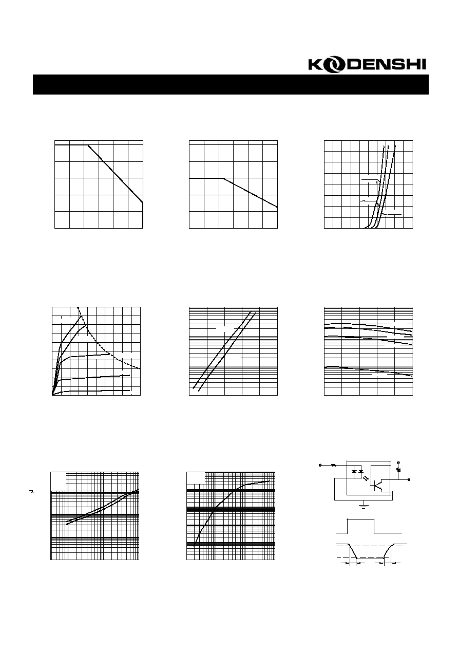
Ambient Temperature Ta (
)
Forward Current vs.
Ambient Temperature
0
-20 0 20
F
o
r
w
a
r
d
C
u
r
r
e
n
t
I
F
(
m
A
)
10
20
40
30
50
Collector Current vs.
Forward Current
Forward Current I
F
(mA)
40 60 100
0.1 1
C
o
l
l
e
c
t
o
r
C
u
r
r
e
n
t
I
C
(
m
A
)
0.1
1
100
10
Collector-Emitter Voltage
V
CE
(V)
Collector Current vs.
Collector-Emitter Voltage
0 2 4 6
C
o
l
l
e
c
t
o
r
C
u
r
r
e
n
t
I
C
(
m
A
)
8 10
0.1
0.1
Load Resistance
R
L
(
)
1 10
Response Time vs.
Load Resistance
R
e
s
p
o
n
s
e
T
i
m
e
t
r
,
t
f
(
s
)
10
100
80
D
a
r
k
C
u
r
r
e
n
t
I
C
E
O
(
)
Ambient Temperature
T
a
(
)
0
0.001
0.01
40
20
0.1
1
80
60 100
Dark Current vs.
Ambient Temperature
Collector Power Dissipation vs.
Ambient Temperature
C
o
l
l
e
c
t
o
r
P
o
w
e
r
D
i
s
s
i
p
a
t
i
o
n
P
C
(
m
W
)
-20
0
50
100
150
200
250
Ambient Temperature Ta (
)
20
0 60
40 100
80
100
0.001
0.01
10
Forward Current vs.
Forward Voltage
F
o
r
w
a
r
d
C
u
r
r
e
n
t
I
F
(
m
A
)
0
80
2.0
1.6
1.2
0.8
0.4
Forward Voltage
V
F
(V)
20
40
60
140
120
100
10
20
30
40
C
o
l
l
e
c
t
o
r
C
u
r
r
e
n
t
I
C
(
m
A
)
0 40
20 80
60
Ambient Temperature
T
a
(
)
Collector Current vs.
Ambient Temperature
10
0
1
100
Output
Input
Test Circuit
V
IN
R
R
L
V
O
V
CC
Waveform
10%
90%
Switching Time Test Circuit
tr
tf
1
500
-20
T
a
=70
T
a
=25
T
a
=-55
T
a
=25
I
F
=30mA
I
F
=20mA
I
F
=10mA
I
F
=5mA
I
F
=1mA
P
C
(max.)
V
CE
=24V
V
CE
=10V
I
F
=20mA
I
F
=10mA
I
F
=5mA
I
F
=1mA
T
a
=25
V
CC
=10V
tr
tf
V
CE
=5V
I
C
=2mA
T
a
=25