FEATURES
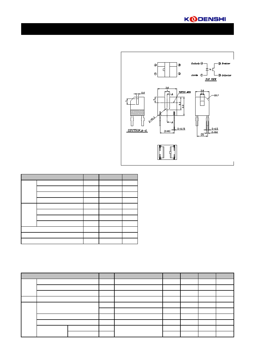
∑ PWB direct mount type
∑ GAP : 1.0mm
APPLICATIONS
∑ Cameras
∑ Floppy disk drives
ABSOLUTE MAXIMUM RATINGS
(Ta=25
)
ELECTRO-OPTICAL CHARACTERISTICS
(Ta=25
)
1/2
-
mA
Light Current (Collect Current)
∑ Encoders
I
L2
V
CE
=5V, I
F
= 5mA (Non-shading)
0.2
Parameter
940
-
Photointerrupter(Transmissive)
KIT-1001A
KIT-1001A combines a high-output GaAs IRED with
DIMENSIONS
The photointerrupter high-performance standard type
75
mA
Reverse Current
260
T
SOL
Soldering Temperature
*3
*1. Pulse width : tw
100
sec.period : T=10msec
*3. For MAX. 5 seconds at the position of 1mm from the package
V
R
=5V
*2. No icebound or dew
Conditions
I
F
=20mA
Collector Current
Storage Temperature
*2
T
STG
Collector Power Dissipation
Operating Temperature
*2
T
OPR
I
C
Parameter
I
F
V
R
I
FP
P
C
V
CEO
V
ECO
Symbol
Input
Output
Forward Current
Reverse Voltage
Pulse Forward Current
*1
Power Dissipation
Collector Emitter Voltage
P
D
Emitter Collector Voltage
V
V
-30 ~ +100
mW
-20 ~ +85
30
5
20
Rating
5
0.5
50
Dark Current
Input
Peak Wavelength
Symbol
V
F
Output
P
I
CEO
I
R
Forward Voltage
Coupled
Rise Time
Collector Emitter Saturation Voltage
Response Time
Fall Time
Leakage Current
tr
tf
I
L1
V
CE(SAT)
I
CEOD
V
CE
=5V, I
C
=1mA,
R
L
=100
-
-
10
-
µs
µs
V
0.15
-
0.4
10
I
F
=20mA
TYP.
1.2
I
F
=10mA, I
C
=0.3mA
-
-
-
MIN.
V
CE
=5V, I
F
=10mA (shading)
-
V
CE
=5V, I
F
=10mA (Non-shading)
-
1
-
0.5
V
CE
=10V, 0lx
-
100
DESCRIPTION
a high sensitivity phototransistor.
∑ Ultra - compact
10
Unit
75
mW
mA
V
A
nA
mA
nm
-
-
1.4
-
Unit
V
MAX.
A
10
0.5
A
Photointerrupter(Transmissive)
2/2
KIT-1001A
()
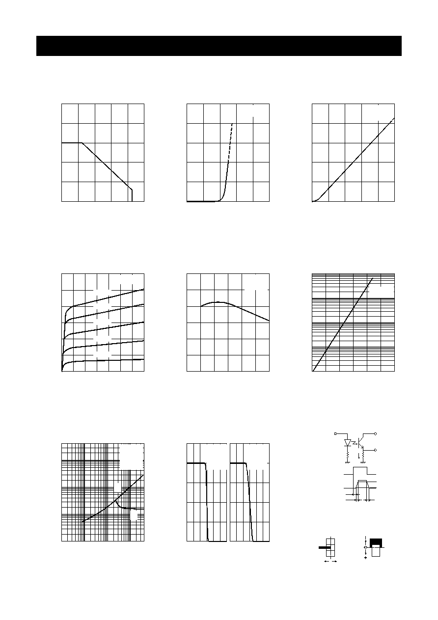
3
2
1
4
10
10
10
10
Relative light current(I )
1
10
Response time tr, tf
Road Resistance(R )
2
10
( )
3
10
4
10
L
-2
0
Moving distance(L)
0
+2
0
-2
(mm)
+2
Collector-Emitter Voltage(V )
10
2
10
3
()
Light Current(I )
0
0
1
2
3
2
4
()
L
4
5
100
Power dissipation(P )
0
0
20
50
()
C
-20
Ambient temperature(Ta)
CE
L
50
100
(%) X
(V)
6
8
12
10
Relative light current(I )
0
0
50
L
100
(%)
Y
0
20
40
Collector dark current(I )
()
60
CEO
(nA)
100
()
40
60
80
0
0
50
()
2.0
F
Forward voltage(V )
0.5
1.0
1.5
(V)
Light Current(I )
L
Method of measuring position
detection characteristic
Optical Axis(X)
0
Optical Axis(Y)
Ambient temperature(Ta)
Response time measurement circuit
Output
Input
td
tr
C
I
Input
V
90%
tf
10%
R
L
OUT
V
CC
0
-1
20
0
1
40
60
2
80 100 ()
30
Forward Current(I )
0
0
10
20
(mA)
F
40
Ambient temperature(Ta)
Forward current(I
F
)
Light Current( I
L
)
Relative light current( I
L
)
Collector dark current( I
CEO
)
Response time tr, tf
Relative light current( I
L
)
Power dissipartion( P
C
)
Forward current( I
F
)
Light Current( I
L
)
Ambient temperature(Ta)
Forward voltage( V
F
)
Forward Current( I
F
)
Collector-Emitter Voltage( V
CE
)
Ambient temperature( Ta )
Ambient temperature( Ta )
Load Resistance( R
L
)
Moving distance( L )
Collector power dissipation Vs.
Ambient temparature
Forward current Vs.
Forward voltage
Light current Vs.
Forward current
Light current Vs.
Collentor-Emitter voltage
Relative light current Vs.
Ambient temperature
Dark current Vs.
Ambient temperature
Switching time Vs.
Load resistance
Relative light current Vs.
Moving distance
Method of measuring position
detection characteristic
Optical Axis(X)
Optical Axis(Y)
Response time measurement circuit
V
CE
=5V
Ta=25
V
CE
=5V
I
F
=20
V
CE
=10V
Ta=25
Ta=25
V
CE
=5V
I
F
=20
Ta=25
V
CE
=5V
I
F
=20
Ta=25
V
CE
=5V
I
C
=2
Ta=25
tr
tf
I
F
=10
I
F
=30
I
F
=40
I
F
=50
I
F
=20