 | –≠–ª–µ–∫—Ç—Ä–æ–Ω–Ω—ã–π –∫–æ–º–ø–æ–Ω–µ–Ω—Ç: 10321111 | –°–∫–∞—á–∞—Ç—å:  PDF PDF  ZIP ZIP |
Specifications
ispLSI and pLSI 1032
1
1996 ISP Encyclopedia
1032_02
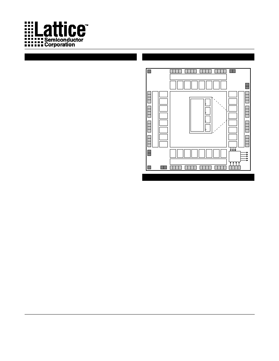
Functional Block Diagram
Output Routing Pool
Output Routing Pool
D7 D6 D5 D4 D3 D2 D1 D0
B0 B1 B2 B3 B4 B5 B6 B7
A0
A1
A2
A3
A4
A5
A6
A7
C7
C6
C5
C4
C3
C2
C1
C0
Output Routing Pool
CLK
Output Routing Pool
Global Routing Pool (GRP)
Logic
Array
D Q
D Q
D Q
D Q
GLB
Description
The ispLSI and pLSI 1032 are High-Density Program-
mable Logic Devices containing 192 Registers, 64
Universal I/O pins, eight Dedicated Input pins, four Dedi-
cated Clock Input pins and a Global Routing Pool (GRP).
The GRP provides complete interconnectivity between
all of these elements. The ispLSI 1032 features 5-Volt in-
system programming and in-system diagnostic
capabilities. It is the first device which offers non-volatile
"on-the-fly" reprogrammability of the logic, as well as the
interconnect to provide truly reconfigurable systems. It is
architecturally and parametrically compatible to the pLSI
1032 device, but multiplexes four of the dedicated input
pins to control in-system programming.
The basic unit of logic on the ispLSI and pLSI 1032
devices is the Generic Logic Block (GLB). The GLBs are
labeled A0, A1 .. D7 (see figure 1). There are a total of
32 GLBs in the ispLSI and pLSI 1032 devices. Each GLB
has 18 inputs, a programmable AND/OR/XOR array, and
four outputs which can be configured to be either combi-
natorial or registered. Inputs to the GLB come from the
GRP and dedicated inputs. All of the GLB outputs are
brought back into the GRP so that they can be connected
to the inputs of any other GLB on the device.
Features
∑ HIGH-DENSITY PROGRAMMABLE LOGIC
-- High Speed Global Interconnect
-- 6000 PLD Gates
-- 64 I/O Pins, Eight Dedicated Inputs
-- 192 Registers
-- Wide Input Gating for Fast Counters, State
Machines, Address Decoders, etc.
-- Small Logic Block Size for Fast Random Logic
-- Security Cell Prevents Unauthorized Copying
∑ HIGH PERFORMANCE E
2
CMOS
Æ
TECHNOLOGY
--
f
max = 90 MHz Maximum Operating Frequency
--
f
max = 60 MHz for Industrial and Military/883 Devices
--
t
pd = 12 ns Propagation Delay
-- TTL Compatible Inputs and Outputs
-- Electrically Erasable and Reprogrammable
-- Non-Volatile E
2
CMOS Technology
-- 100% Tested
∑ ispLSI OFFERS THE FOLLOWING ADDED FEATURES
-- In-System ProgrammableTM (ISPTM) 5-Volt Only
-- Increased Manufacturing Yields, Reduced Time-to-
Market, and Improved Product Quality
-- Reprogram Soldered Devices for Faster Prototyping
∑ COMBINES EASE OF USE AND THE FAST SYSTEM
SPEED OF PLDs WITH THE DENSITY AND FLEX-
IBILITY OF FIELD PROGRAMMABLE GATE ARRAYS
-- Complete Programmable Device Can Combine Glue
Logic and Structured Designs
-- Four Dedicated Clock Input Pins
-- Synchronous and Asynchronous Clocks
-- Flexible Pin Placement
-- Optimized Global Routing Pool Provides Global
Interconnectivity
∑ ispLSI AND pLSI DEVELOPMENT TOOLS
pDS
Æ
Software
-- Easy to Use PC WindowsTM Interface
-- Boolean Logic Compiler
-- Manual Partitioning
-- Automatic Place and Route
-- Static Timing Table
ispDS+TM Software
-- Industry Standard, Third Party Design
Environments
-- Schematic Capture, State Machine, HDL
-- Automatic Partitioning and Place and Route
-- Comprehensive Logic and Timing Simulation
-- PC and Workstation Platforms
ispLSI
Æ
and pLSI
Æ
1032
High-Density Programmable Logic
Copyright © 1997 Lattice Semiconductor Corp. All brand or product names are trademarks or registered trademarks of their respective holders. The specifications and information herein are subject
to change without notice.
LATTICE SEMICONDUCTOR CORP., 5555 Northeast Moore Ct., Hillsboro, Oregon 97124, U.S.A.
February 1997
Tel. (503) 681-0118; 1-800-LATTICE; FAX (503) 681-3037; http://www.latticesemi.com
1996 ISP Encyclopedia
Specifications
ispLSI and pLSI 1032
2
1996 ISP Encyclopedia
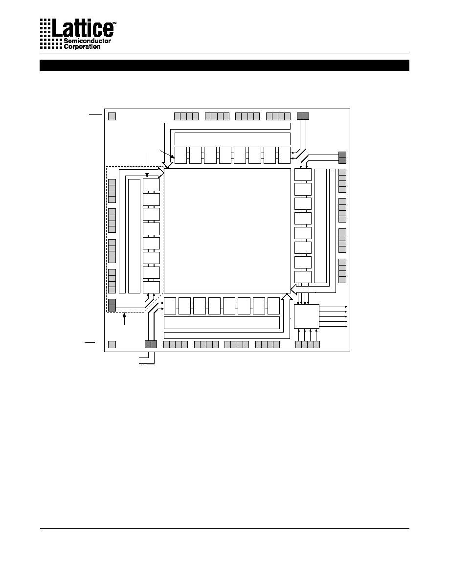
Functional Block Diagram
Figure 1. ispLSI and pLSI 1032 Functional Block Diagram
The devices also have 64 I/O cells, each of which is
directly connected to an I/O pin. Each I/O cell can be
individually programmed to be a combinatorial input,
registered input, latched input, output or bi-directional
I/O pin with 3-state control. Additionally, all outputs are
polarity selectable, active high or active low. The signal
levels are TTL compatible voltages and the output drivers
can source 4 mA or sink 8 mA.
Eight GLBs, 16 I/O cells, two dedicated inputs and one
ORP are connected together to make a Megablock (see
figure 1). The outputs of the eight GLBs are connected to
a set of 16 universal I/O cells by the ORP. The I/O cells
within the Megablock also share a common Output
Enable (OE) signal. The ispLSI and pLSI 1032 devices
contain four of these Megablocks.
The GRP has as its inputs the outputs from all of the GLBs
and all of the inputs from the bi-directional I/O cells. All of
these signals are made available to the inputs of the
GLBs. Delays through the GRP have been equalized to
minimize timing skew.
Clocks in the ispLSI and pLSI 1032 devices are selected
using the Clock Distribution Network. Four dedicated
clock pins (Y0, Y1, Y2 and Y3) are brought into the
distribution network, and five clock outputs (CLK 0, CLK
1, CLK 2, IOCLK 0 and IOCLK 1) are provided to route
clocks to the GLBs and I/O cells. The Clock Distribution
Network can also be driven from a special clock GLB (C0
on the ispLSI and pLSI 1032 devices). The logic of this
GLB allows the user to create an internal clock from a
combination of internal signals within the device.
Y
0
Y
1
Y
2
Y
3
I/O 0
I/O 1
I/O 2
I/O 3
IN 5
IN 4
I/O 6
I/O 7
I/O 8
I/O 9
I/O 10
I/O 11
I/O 12
I/O 13
I/O 14
I/O 15
I/O 47
I/O 46
I/O 45
I/O 44
I/O 43
I/O 42
I/O 41
I/O 40
I/O 39
I/O 38
I/O 37
I/O 36
I/O 35
I/O 34
I/O 33
I/O 32
*SDI/IN 0
*MODE/IN 1
I/O
62
I/O
63
I/O
61
I/O
60
I/O
59
I/O
58
I/O
57
I/O
56
I/O
55
I/O
54
I/O
53
I/O
52
I/O
51
I/O
50
I/O
49
I/O
48
IN
7
IN
6
I/O
17
I/O
16
I/O
18
I/O
19
I/O
20
I/O
21
I/O
22
I/O
23
I/O
24
I/O
25
I/O
26
I/O
27
I/O
28
I/O
29
I/O
30
I/O
31
*SDO/IN 2
*SCLK/IN 3
I/O 4
I/O 5
RESET
Global
Routing
Pool
(GRP)
Output Routing Pool (ORP)
Output Routing Pool (ORP)
CLK 0
CLK 1
CLK 2
IOCLK 0
IOCLK 1
Clock
Distribution
Network
D7
D6
D5
D4
D3
D2
D1
D0
B0
B1
B2
B3
B4
B5
B6
B7
A0
A1
A2
A3
A4
A5
A6
A7
C7
C6
C5
C4
C3
C2
C1
C0
Output Routing Pool (ORP)
Generic
Logic Blocks
(GLBs)
Megablock
Output Routing Pool (ORP)
Input Bus
Input Bus
Input Bus
*ispEN/NC
lnput Bus
*ISP Control Functions for ispLSI 1032 Only
0139(1)-32-isp
Specifications
ispLSI and pLSI 1032
3
1996 ISP Encyclopedia
Absolute Maximum Ratings
1
Supply Voltage V
cc
................................... -0.5 to +7.0V
Input Voltage Applied ........................ -2.5 to V
CC
+1.0V
Off-State Output Voltage Applied ..... -2.5 to V
CC
+1.0V
Storage Temperature ................................ -65 to 150
∞
C
Case Temp. with Power Applied .............. -55 to 125
∞
C
Max. Junction Temp. (T
J
) with Power Applied ... 150
∞
C
1. Stresses above those listed under the "Absolute Maximum Ratings" may cause permanent damage to the device. Functional
operation of the device at these or at any other conditions above those indicated in the operational sections of this specifica tion
is not implied (while programming, follow the programming specifications).
DC Recommended Operating Conditions
V
V
PARAMETER
SYMBOL
MIN.
MAX.
UNITS
5.25
5.5
5.5
0.8
Vcc + 1
Supply Voltage
V
CC
V
IL
V
IH
Table 2- 0005Aisp w/mil.eps
4.75
4.5
4.5
0
2.0
Commercial T
A
=
0
∞
C to +70
∞
C
Industrial
T
A
= -40
∞
C to +85
∞
C
Military/883
T
C
= -55
∞
C to +125
∞
C
Input Low Voltage
Input High Voltage
V
Capacitance (T
A
=25
o
C, f=1.0 MHz)
SYMBOL
PARAMETER
MAXIMUM
1
UNITS
TEST CONDITIONS
C
1
Commercial/Industrial
8
pf
V
CC
=5.0V, V
IN
=2.0V
Military
10
pf
V
CC
=5.0V, V
IN
=2.0V
C
2
I/O and Clock Capacitance
10
pf
V
CC
=5.0V, V
I/O
, V
Y
=2.0V
1
.
Guaranteed but not 100% tested.
Table 2- 0006
Dedicated Input Capacitance
Data Retention Specifications
Table 2- 0008B
PARAMETER
pLSI Erase/Reprogram Cycles
100
Data Retention
MINIMUM
MAXIMUM
UNITS
ispLSI Erase/Reprogram Cycles
20
10000
≠
≠
≠
Cycles
Years
Cycles
Specifications
ispLSI and pLSI 1032
4
1996 ISP Encyclopedia
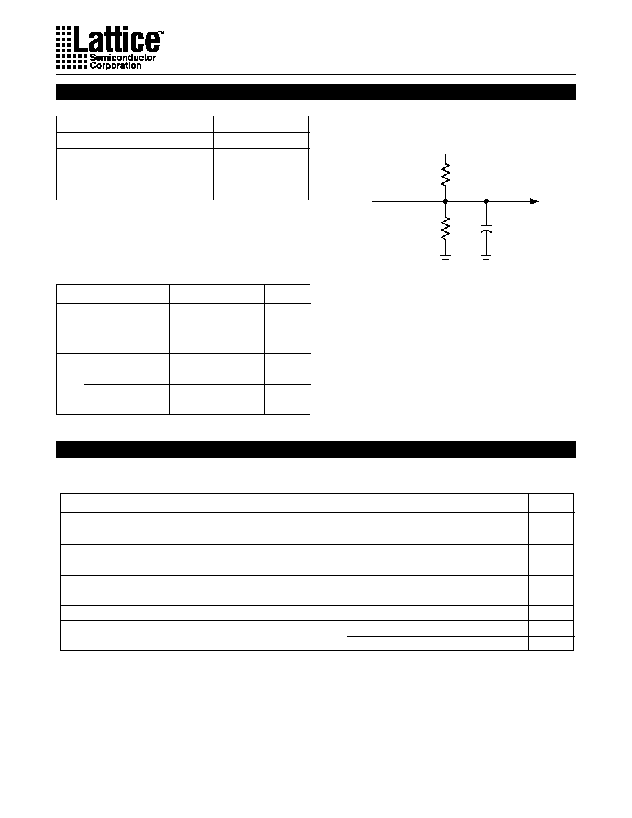
Switching Test Conditions
Input Pulse Levels
GND to 3.0V
Input Rise and Fall Time
3ns 10% to 90%
Input Timing Reference Levels
1.5V
Output Timing Reference Levels
1.5V
Output Load
See figure 2
3-state levels are measured 0.5V from steady-state
active level.
Table 2- 0003
Output Load Conditions (see figure 2)
Test Condition
R1
R2
CL
A
470
390
35pF
B
Active High
390
35pF
Active Low
470
390
35pF
Active High to Z
390
5pF
C
at V
OH
- 0.5V
Active Low to Z
470
390
5pF
at V
OL
+ 0.5V
Figure 2. Test Load
+ 5V
R1
R2
CL
*
Device
Output
Test
Point
*
CL includes Test Fixture and Probe Capacitance.
DC Electrical Characteristics
Over Recommended Operating Conditions
0.4
≠
-10
10
-150
-150
-200
190
220
V
V
µ
A
µ
A
µ
A
µ
A
mA
mA
mA
SYMBOL
V
OL
V
OH
I
IL
I
IH
I
IL-isp
I
IL-PU
I
OS
1
I
CC
2,4
Output Low Voltage
Output High Voltage
Input or I/O Low Leakage Current
Input or I/O High Leakage Current
isp Input Low Leakage Current
I/O Active Pull-Up Current
Output Short Circuit Current
Operating Power Supply Current
I
OL
=8 mA
I
OH
=-4 mA
0V
V
IN
V
IL
(MAX.)
3.5V
V
IN
V
CC
0V
V
IN
V
IL
(MAX.)
0V
V
IN
V
IL
V
CC
= 5V, V
OUT
= 0.5V
V
IL
= 0.5V, V
IH
= 3.0V Commercial
f
TOGGLE
= 1 MHz
Industrial/Military
PARAMETER
CONDITION
MIN.
UNITS
MAX.
TYP.
3
≠
≠
≠
≠
≠
≠
≠
130
135
≠
2.4
≠
≠
≠
≠
≠
≠
≠
1. One output at a time for a maximum duration of one second.
2. Measured using eight 16-bit counters.
3. Typical values are at V
CC
= 5V and T
A
= 25
o
C.
4. Maximum I
CC
varies widely with specific device configuration and operating frequency. Refer to the Power Consumption sec-
tion of this datasheet and Thermal Management section of this Data Book to estimate maximum I
CC
.
Table 2- 0007A-32-isp

Specifications
ispLSI and pLSI 1032
5
1996 ISP Encyclopedia
USE 1032E-80
FOR NEW DESIGNS
USE 1032E-70
FOR NEW DESIGNS
External Timing Parameters
Over Recommended Operating Conditions
1. Unless noted otherwise, all parameters use a GRP load of 4 GLBs, ORP and Y0 clock.
2. Refer to Timing Model in this data sheet for further details.
3. Standard 16-Bit counter using GRP feedback.
4. fmax (Toggle) may be less than 1/(twh + twl). This is to allow for a clock duty cycle of other than 50%.
5. Reference Switching Test Conditions section.
MIN. MAX.
Data Propagation Delay, 4PT bypass, ORP bypass
Data Propagation Delay, Worst Case Path
Clock Frequency with Internal Feedback
3
Clock Frequency with External Feedback
Clock Frequency, Max Toggle
4
GLB Reg. Setup Time before Clock, 4PT bypass
GLB Reg. Clock to Output Delay, ORP bypass
GLB Reg. Hold Time after Clock, 4 PT bypass
GLB Reg. Setup Time before Clock
GLB Reg. Clock to Output Delay
GLB Reg. Hold Time after Clock
Ext. Reset Pin to Output Delay
Ext. Reset Pulse Duration
Input to Output Enable
Input to Output Disable
Ext. Sync. Clock Pulse Duration, High
Ext. Sync. Clock Pulse Duration, Low
I/O Reg. Setup Time before Ext. Sync. Clock (Y2, Y3)
I/O Reg. Hold Time after Ext. Sync. Clock (Y2, Y3)
ns
ns
MHz
MHz
MHz
ns
ns
ns
ns
ns
ns
ns
ns
ns
ns
ns
ns
ns
ns
t
pd1
t
pd2
f
max (Int.)
f
max (Ext.)
f
max (Tog.)
t
su1
t
co1
t
h1
t
su2
t
co2
t
h2
t
r1
t
rw1
t
en
t
dis
t
wh
t
wl
t
su5
t
h5
1
2
3
4
5
6
7
8
9
10
11
12
13
14
15
16
17
18
19
A
A
A
≠
≠
≠
A
≠
≠
≠
≠
A
≠
B
C
≠
≠
≠
≠
DESCRIPTION
1
PARAMETER
#
2
UNITS
TEST
5
COND.
1
tsu2 + tco1
( )
MIN. MAX.
≠
≠
80
50
100
7
≠
0
10
≠
0
≠
10
≠
≠
5
5
2
6.5
15
20
≠
≠
≠
≠
10
≠
≠
12
≠
17
≠
18
18
≠
≠
≠
≠
≠
≠
60
38
83
9
≠
0
13
≠
0
≠
13
≠
≠
6
6
2.5
8.5
20
25
≠
≠
≠
≠
13
≠
≠
16
≠
22.5
≠
24
24
≠
≠
≠
≠
-80
-60
MIN. MAX.
≠
≠
90.9
58.8
125
6
≠
0
9
≠
0
≠
10
≠
≠
4
4
2
6.5
12
17
≠
≠
≠
≠
8
≠
≠
10
≠
15
≠
15
15
≠
≠
≠
≠
-90
Table 2-0030-32/90,80,60C