 | –≠–ª–µ–∫—Ç—Ä–æ–Ω–Ω—ã–π –∫–æ–º–ø–æ–Ω–µ–Ω—Ç: 2064VE | –°–∫–∞—á–∞—Ç—å:  PDF PDF  ZIP ZIP |
Document Outline
- Table of Contents
- ispLSI 2064VE Data Sheet
- DC Electrical Characteristics
- AC Characteristics
- Signal Configuration: 100 caBGA
- Pin Configuration: 100 TQFP
- Pin Configuration: 44 PLCC
- Pin Configuration: 44 TQFP
- Ordering Information
ispLSI
Æ
2064VE
3.3V In-System Programmable
High Density SuperFASTTM PLD
2064ve_06
1
Features
∑ SuperFAST HIGH DENSITY PROGRAMMABLE LOGIC
-- 2000 PLD Gates
-- 64 and 32 I/O Pin Versions, Four Dedicated Inputs
-- 64 Registers
-- High Speed Global Interconnect
-- Wide Input Gating for Fast Counters, State
Machines, Address Decoders, etc.
-- Small Logic Block Size for Random Logic
-- 100% Functional, JEDEC and Pinout Compatible with
ispLSI 2064V Devices
∑ 3.3V LOW VOLTAGE 2064 ARCHITECTURE
-- Interfaces with Standard 5V TTL Devices
∑ HIGH-PERFORMANCE E
2
CMOS
Æ
TECHNOLOGY
--
f
max = 280MHz* Maximum Operating Frequency
--
t
pd = 3.5ns* Propagation Delay
-- Electrically Erasable and Reprogrammable
-- Non-Volatile
-- 100% Tested at Time of Manufacture
-- Unused Product Term Shutdown Saves Power
∑ IN-SYSTEM PROGRAMMABLE
-- 3.3V In-System Programmability (ISPTM) Using
Boundary Scan Test Access Port (TAP)
-- Open-Drain Output Option for Flexible Bus Interface
Capability, Allowing Easy Implementation of Wired-OR
or Bus Arbitration Logic
-- Increased Manufacturing Yields, Reduced Time-to-
Market and Improved Product Quality
-- Reprogram Soldered Devices for Faster Prototyping
∑ 100% IEEE 1149.1 BOUNDARY SCAN TESTABLE
∑ THE EASE OF USE AND FAST SYSTEM SPEED OF
PLDs WITH THE DENSITY AND FLEXIBILITY OF FPGAs
-- Enhanced Pin Locking Capability
-- Three Dedicated Clock Input Pins
-- Synchronous and Asynchronous Clocks
-- Programmable Output Slew Rate Control
-- Flexible Pin Placement
-- Optimized Global Routing Pool Provides Global
Interconnectivity
∑ ispDesignEXPERTTM ≠ LOGIC COMPILER AND COM-
PLETE ISP DEVICE DESIGN SYSTEMS FROM HDL
SYNTHESIS THROUGH IN-SYSTEM PROGRAMMING
-- Superior Quality of Results
-- Tightly Integrated with Leading CAE Vendor Tools
-- Productivity Enhancing Timing Analyzer, Explore
Tools, Timing Simulator and ispANALYZERTM
-- PC and UNIX Platforms
*Advanced Information
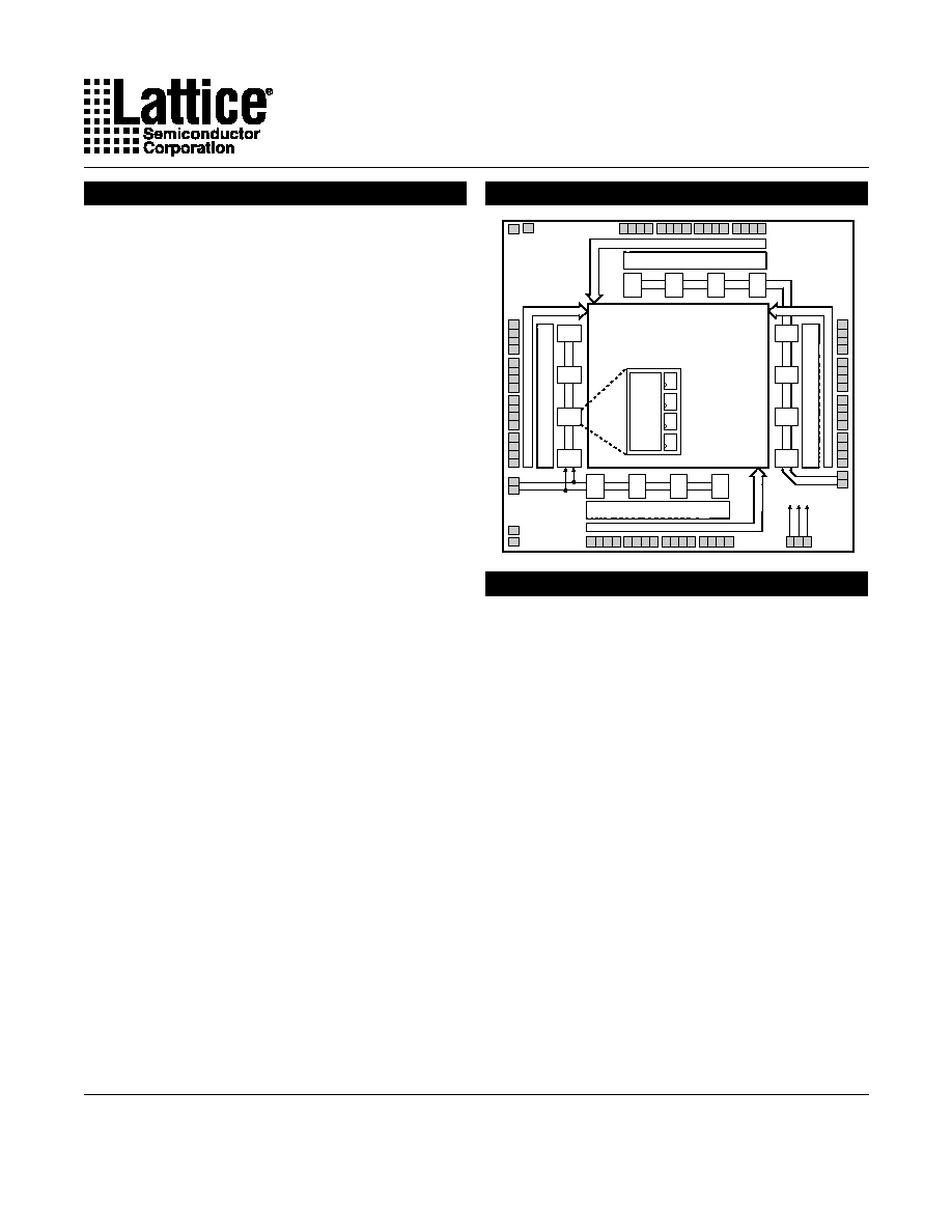
Functional Block Diagram
Global Routing Pool
(GRP)
A0
A1
A3
Input Bus
Output Routing Pool (ORP)
B3
B2
B1
B0
Input Bus
Output Routing Pool (ORP)
A2
GLB
Logic
Array
D Q
D Q
D Q
D Q
A4
A5
A6
A7
B7
B6
B5
B4
Input Bus
Output Routing Pool (ORP)
Input Bus
Output Routing Pool (ORP)
0139A/2064V
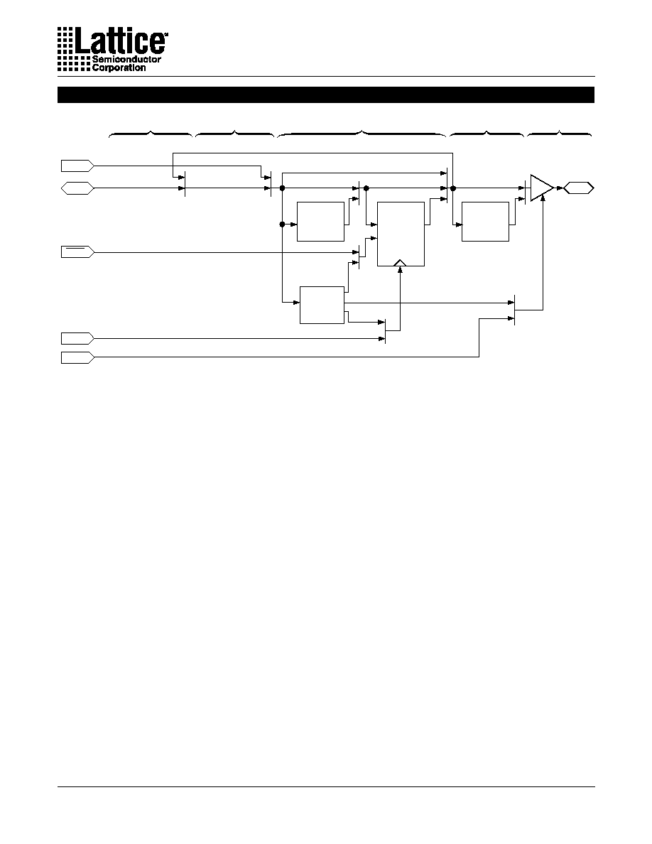
Description
The ispLSI 2064VE is a High Density Programmable
Logic Device available in 64 and 32 I/O-pin versions. The
device contains 64 Registers, four Dedicated Input pins,
three Dedicated Clock Input pins, two dedicated Global
OE input pins and a Global Routing Pool (GRP). The
GRP provides complete interconnectivity between all of
these elements. The ispLSI 2064VE features in-system
programmability through the Boundary Scan Test Ac-
cess Port (TAP) and is 100% IEEE 1149.1 Boundary
Scan Testable. The ispLSI 2064VE offers non-volatile
reprogrammability of the logic, as well as the intercon-
nect, to provide truly reconfigurable systems.
The basic unit of logic on the ispLSI 2064VE device is the
Generic Logic Block (GLB). The GLBs are labeled A0,
A1...B7 (see Figure 1). There are a total of 16 GLBs in the
ispLSI 2064VE device. Each GLB is made up of four
macrocells. Each GLB has 18 inputs, a programmable
AND/OR/Exclusive OR array, and four outputs which can
be configured to be either combinatorial or registered.
Inputs to the GLB come from the GRP and dedicated
inputs. All of the GLB outputs are brought back into the
GRP so that they can be connected to the inputs of any
GLB on the device.
Copyright © 2000 Lattice Semiconductor Corp. All brand or product names are trademarks or registered trademarks of their respective holders. The specifications and information herein are subject
to change without notice.
LATTICE SEMICONDUCTOR CORP., 5555 Northeast Moore Ct., Hillsboro, Oregon 97124, U.S.A.
September 2000
Tel. (503) 268-8000; 1-800-LATTICE; FAX (503) 268-8556; http://www.latticesemi.com
2
Specifications
ispLSI 2064VE
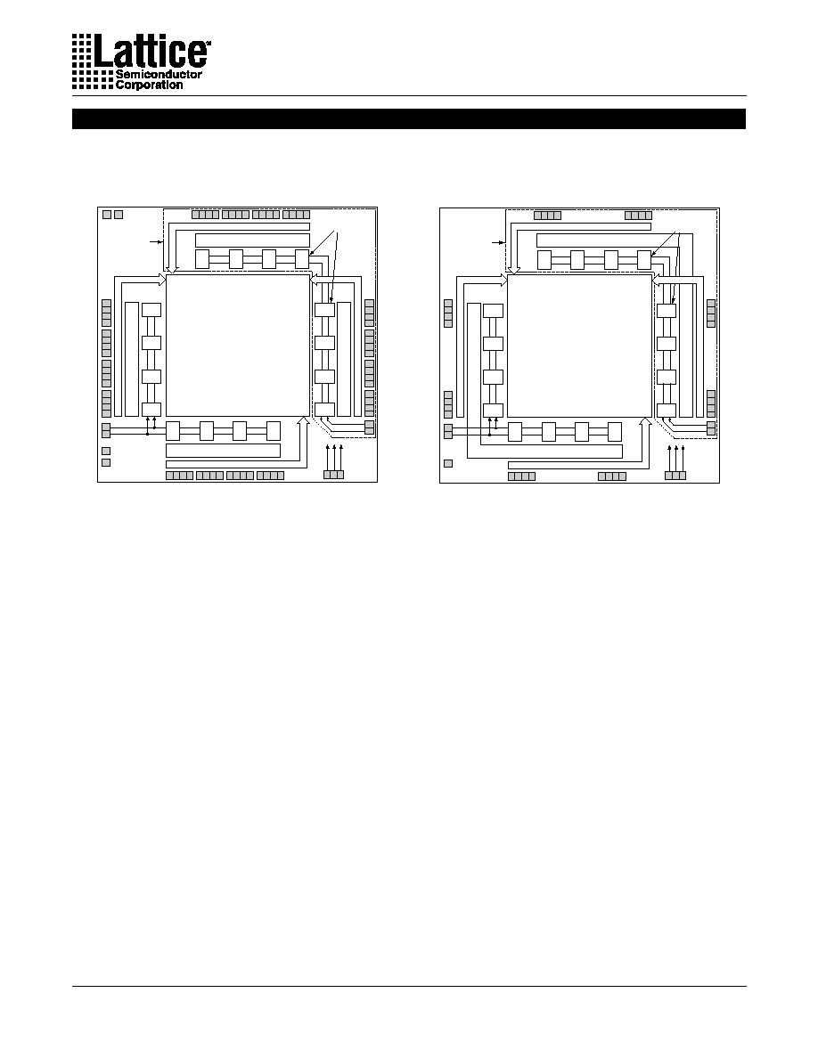
Functional Block Diagram
Figure 1. ispLSI 2064VE Functional Block Diagram (64-I/O and 32-I/O Versions)
The 64-I/O 2064VE contains 64 I/O cells, while the 32-
I/O version contains 32 I/O cells. Each I/O cell is directly
connected to an I/O pin and can be individually pro-
grammed to be a combinatorial input, output or
bi-directional I/O pin with 3-state control. The signal
levels are TTL compatible voltages and the output drivers
can source 4 mA or sink 8 mA. Each output can be
programmed independently for fast or slow output slew
rate to minimize overall output switching noise. Device
pins can be safely driven to 5-Volt signal levels to support
mixed-voltage systems.
Eight GLBs, 32 or 16 I/O cells, two dedicated inputs and
two or one ORPs are connected together to make a
Megablock (see Figure 1). The outputs of the eight GLBs
are connected to a set of 32 or 16 universal I/O cells by
two or one ORPs. Each ispLSI 2064VE device contains
two Megablocks.
The GRP has as its inputs, the outputs from all of the
GLBs and all of the inputs from the bi-directional I/O cells.
All of these signals are made available to the inputs of the
GLBs. Delays through the GRP have been equalized to
minimize timing skew.
Clocks in the ispLSI 2064VE device are selected using
the dedicated clock pins. Three dedicated clock pins (Y0,
TDO/IN 2
Global Routing Pool
(GRP)
A0
A1
A3
Input Bus
Output Routing Pool (ORP)
B3
B2
B1
B0
Input Bus
Output Routing Pool (ORP)
A2
CLK 0
CLK 1
CLK 2
GOE 0
I/O 0
I/O 1
I/O 2
I/O 3
I/O 6
I/O 7
I/O 8
I/O 9
I/O 10
I/O 11
I/O 12
I/O 13
I/O 14
I/O 15
I/O 47
I/O 46
I/O 45
I/O 44
I/O 43
I/O 42
I/O 41
I/O 40
I/O 39
I/O 38
I/O 37
I/O 36
I/O 35
I/O 34
I/O 33
I/O 32
TDI/IN 0
TMS/IN 1
I/O 4
I/O 5
BSCAN
RESET
0139B/2064VE
I/O 63
I/O 62
I/O 61
I/O 60
I/O 59
I/O 58
I/O 57
I/O 56
I/O 55
I/O 54
I/O 53
I/O 52
I/O 51
I/O 50
I/O 49
I/O 48
Input Bus
Output Routing Pool (ORP)
I/O 16
I/O 17
I/O 18
I/O 19
I/O 20
I/O 21
I/O 22
I/O 23
I/O 24
I/O 25
I/O 26
I/O 27
I/O 28
I/O 29
I/O 30
Y0
Y1
Y2
I/O 31
Output Routing Pool (ORP)
Megablock
Input Bus
A4
A5
A6
A7
B7
B6
B5
B4
GOE 1
TCK/IN 3
Generic Logic
Blocks (GLBs)
Y1, Y2) or an asynchronous clock can be selected on a
GLB basis. The asynchronous or Product Term clock
can be generated in any GLB for its own clock.
Programmable Open-Drain Outputs
In addition to the standard output configuration, the
outputs of the ispLSI 2064VE are individually program-
mable, either as a standard totem-pole output or an
open-drain output. The totem-pole output drives the
specified Voh and Vol levels, whereas the open-drain
output drives only the specified Vol. The Voh level on the
open-drain output depends on the external loading and
pull-up. This output configuration is controlled by a pro-
grammable fuse. The default configuration when the
device is in bulk erased state is totem-pole configuration.
The open-drain/totem-pole option is selectable through
the ispDesignEXPERT software tools.
TMS/IN 2
Global Routing Pool
(GRP)
A0
A1
A3
Input Bus
Output Routing Pool (ORP)
B3
B2
B1
B0
Output Routing Pool (ORP)
A2
CLK 0
CLK 1
CLK 2
I/O 0
I/O 1
I/O 2
I/O 3
I/O 6
I/O 7
I/O 8
I/O 9
I/O 10
I/O 11
I/O 12
I/O 13
I/O 14
I/O 15
I/O 23
I/O 22
I/O 21
I/O 20
I/O 19
I/O 18
I/O 17
I/O 16
TDI/IN 0
TDO/IN 1
I/O 4
I/O 5
BSCAN
0139B/2064VE.32IO
I/O 31
I/O 30
I/O 29
I/O 28
I/O 27
I/O 26
I/O 25
I/O 24
Input Bus
Output Routing Pool (ORP)
GOE1/Y0
RESET
/Y1
TCK/Y2
Output Routing Pool (ORP)
Megablock
Input Bus
A4
A5
A6
A7
B7
B6
B5
B4
GOE0/IN 3
Generic Logic
Blocks (GLBs)
Input Bus
3
Specifications
ispLSI 2064VE
C
SYMBOL
Table 2-0006/2064VE
C
PARAMETER
I/O Capacitance
6
UNITS
TYPICAL
TEST CONDITIONS
1
2
8
Dedicated Input Capacitance
pf
pf
V = 3.3V, V = 0.0V
V = 3.3V, V = 0.0V
CC
CC
I/O
IN
C
Clock and Global Output Enable Capacitance
10
3
pf
V = 3.3V, V = 0.0V
CC
Y
Absolute Maximum Ratings
1
Supply Voltage V
cc ...................................................
-0.5 to +5.4V
Input Voltage Applied ..................................... -0.5 to +5.6V
Off-State Output Voltage Applied .................. -0.5 to +5.6V
Storage Temperature ..................................... -65 to 150
∞
C
Case Temp. with Power Applied .................... -55 to 125
∞
C
Max. Junction Temp. (T
J
) with Power Applied ............ 150
∞
C
1. Stresses above those listed under the "Absolute Maximum Ratings" may cause permanent damage to the device. Functional
operation of the device at these or at any other conditions above those indicated in the operational sections of this specification
is not implied (while programming, follow the programming specifications).
DC Recommended Operating Condition
Capacitance (TA=25
∞
C, f=1.0 MHz)
Table 2-0008/2064VE
PARAMETER
MINIMUM
MAXIMUM
UNITS
Erase/Reprogram Cycles
10000
≠
Cycles
Erase Reprogram Specifications
T
A
= 0
∞
C to + 70
∞
C
T
A
= -40
∞
C to + 85
∞
C
SYMBOL
Table 2-0005/2064V
V
CC
V
IH
V
IL
PARAMETER
Supply Voltage
Input High Voltage
Input Low Voltage
MIN.
MAX.
UNITS
3.0
3.0
2.0
V ≠ 0.5
3.6
3.6
5.25
0.8
V
V
V
V
SS
Commercial
Industrial
4
Specifications
ispLSI 2064VE
Switching Test Conditions
+ 3.3V
R1
R2
CL
*
Device
Output
Test
Point
*
CL includes Test Fixture and Probe Capacitance.
0213A/2064V
Figure 2. Test Load
DC Electrical Characteristics
Over Recommended Operating Conditions
V
OL
SYMBOL
1. One output at a time for a maximum duration of one second. V = 0.5V was selected to avoid test
problems by tester ground degradation. Characterized but not 100% tested.
2. Measured using four 16-bit counters.
3. Typical values are at V = 3.3V and T = 25
∞
C.
4. Maximum I varies widely with specific device configuration and operating frequency. Refer to the Power Consumption
section of this data sheet and Thermal Management section of the Lattice Semiconductor Data Book or CD-ROM to
estimate maximum I .
Table 2-0007/2064VE
1
V
OH
I
IH
I
IL
I
IL-isp
PARAMETER
I
IL-PU
I
OS
2, 4
I
CC
Output Low Voltage
Output High Voltage
Input or I/O High Leakage Current
Input or I/O Low Leakage Current
BSCAN Input Low Leakage Current
I/O Active Pull-Up Current
Output Short Circuit Current
Operating Power Supply Current
I = 8 mA
I = -4 mA
0V
V
V (Max.)
0V
V
V
0V
V
V
V = 3.3V, V = 0.5V
V = 0.0V, V = 3.0V
f = 1 MHz
OL
OH
IN IL
IN
IL
IN IL
CC OUT
CLOCK
IL
IH
CONDITION
MIN.
TYP.
MAX.
UNITS
3
≠
2.4
≠
≠
≠
≠
≠
≠
≠
≠
90
≠
≠
≠
≠
≠
≠
≠
0.4
≠
10
10
-10
-150
-150
-100
≠
V
V
µ
A
µ
A
µ
A
µ
A
µ
A
mA
mA
CC
A
OUT
CC
CC
(V ≠ 0.2)V
V
V
V
V
5.25V
IN
CC
CC
IN
CC
Input Pulse Levels
Table 2-0003/2064VE
Input Rise and Fall Time
Input Timing Reference Levels
Output Timing Reference Levels
Output Load
GND to 3.0V
1.5V
1.5V
See Figure 2
3-state levels are measured 0.5V from
steady-state active level.
1.5 ns 10% to 90%
TEST CONDITION
R1
R2
CL
A
316
348
35pF
B
348
35pF
316
348
35pF
Active High
Active Low
C
316
348
5pF
348
5pF
Active Low to Z
at V +0.5V
OL
Active High to Z
at V -0.5V
OH
Table 2-0004/2064V
Output Load Conditions (see Figure 2)

5
Specifications
ispLSI 2064VE
A
D
V
A
N
C
E
D
IN
F
O
R
M
A
T
IO
N
External Timing Parameters
Over Recommended Operating Conditions
t
pd1
UNITS
TEST
COND.
1. Unless noted otherwise, all parameters use a GRP load of four, 20 PTXOR path, ORP and Y0 clock.
2. Standard 16-bit counter using GRP feedback.
3. Reference Switching Test Conditions section.
Table 2-0030A/2064VE
1
3
2
1
tsu2 + tco1
( )
DESCRIPTION
#
PARAMETER
A
1
Data Propagation Delay, 4PT Bypass, ORP Bypass
ns
t
pd2
A
2
Data Propagation Delay
ns
f
max
A
3
Clock Frequency with Internal Feedback
MHz
f
max (Ext.)
--
4
Clock Frequency with External Feedback
MHz
f
max (Tog.)
--
5
Clock Frequency, Max. Toggle
MHz
t
su1
--
6
GLB Reg. Setup Time before Clock, 4 PT Bypass
ns
t
co1
A
7
GLB Reg. Clock to Output Delay, ORP Bypass
ns
t
h1
--
8
GLB Reg. Hold Time after Clock, 4 PT Bypass
ns
t
su2
--
9
GLB Reg. Setup Time before Clock
ns
t
co2
A
10
GLB Reg. Clock to Output Delay
ns
t
h2
--
11
GLB Reg. Hold Time after Clock
ns
t
r1
A
12
Ext. Reset Pin to Output Delay
ns
t
rw1
--
13
Ext. Reset Pulse Duration
ns
t
ptoeen
B
14
Input to Output Enable
ns
t
ptoedis
C
15
Input to Output Disable
ns
t
goeen
B
16
Global OE Output Enable
ns
t
goedis
C
17
Global OE Output Disable
ns
t
wh
--
18
External Synchronous Clock Pulse Duration, High
ns
t
wl
--
19
External Synchronous Clock Pulse Duration, Low
ns
-200
MIN. MAX.
--
4.5
--
200
--
--
--
--
--
0.0
4.0
--
0.0
--
4.0
--
--
--
--
2.5
--
2.5
--
133
200
3.0
3.5
--
--
4.5
--
6.0
--
8.0
8.0
5.0
5.0
7.0
-280
MIN. MAX.
--
3.5
--
280
--
--
--
--
--
--
--
--
--
--
--
--
--
--
--
--
--
--
--
--
--
--
--
--
--
--
--
--
--
--
--
--
--
--
6
Specifications
ispLSI 2064VE
External Timing Parameters
Over Recommended Operating Conditions
t
pd1
UNITS
-100
MIN.
TEST
COND.
1. Unless noted otherwise, all parameters use a GRP load of four, 20 PTXOR path, ORP and Y0 clock.
2. Standard 16-bit counter using GRP feedback.
3. Reference Switching Test Conditions section.
Table 2-0030B/2064VE
1
3
2
1
tsu2 + tco1
( )
MAX.
DESCRIPTION
#
PARAMETER
A
1
Data Propagation Delay, 4PT Bypass, ORP Bypass
--
10.0
ns
t
pd2
A
2
Data Propagation Delay
--
ns
f
max
A
3
Clock Frequency with Internal Feedback
100
--
MHz
f
max (Ext.)
--
4
Clock Frequency with External Feedback
--
MHz
f
max (Tog.)
--
5
Clock Frequency, Max. Toggle
--
MHz
t
su1
--
6
GLB Reg. Setup Time before Clock, 4 PT Bypass
--
ns
t
co1
A
7
GLB Reg. Clock to Output Delay, ORP Bypass
--
ns
t
h1
--
8
GLB Reg. Hold Time after Clock, 4 PT Bypass
0.0
ns
t
su2
--
9
GLB Reg. Setup Time before Clock
8.0
ns
t
co2
A
10
GLB Reg. Clock to Output Delay
--
ns
t
h2
--
11
GLB Reg. Hold Time after Clock
0.0
ns
t
r1
A
12
Ext. Reset Pin to Output Delay
--
ns
t
rw1
--
13
Ext. Reset Pulse Duration
6.5
ns
t
ptoeen
B
14
Input to Output Enable
--
ns
t
ptoedis
C
15
Input to Output Disable
--
ns
t
goeen
B
16
Global OE Output Enable
--
ns
t
goedis
C
17
Global OE Output Disable
--
ns
t
wh
--
18
External Synchronous Clock Pulse Duration, High
5.0
--
ns
t
wl
--
19
External Synchronous Clock Pulse Duration, Low
5.0
--
ns
77
100
6.5
5.0
--
--
6.0
--
13.5
--
15.0
15.0
9.0
9.0
13.0
-135
MIN. MAX.
--
7.5
--
135
--
--
--
--
--
0.0
6.0
--
0.0
--
5.0
--
--
--
--
3.5
--
3.5
--
100
143
5.0
4.0
--
--
5.0
--
10.0
--
12.0
12.0
7.0
7.0
10.0
7
Specifications
ispLSI 2064VE
Internal Timing Parameters
1
Over Recommended Operating Conditions
t
io
1. Internal Timing Parameters are not tested and are for reference only.
2. Refer to Timing Model in this data sheet for further details.
3. The XOR adjacent path can only be used by hard macros.
Table 2-0036/2064VE
Inputs
UNITS
-135
-200
MIN.
-100
MIN.
MAX.
MIN. MAX.
MAX.
DESCRIPTION
#
2
PARAMETER
20 Input Buffer Delay
ns
t
din
21 Dedicated Input Delay
ns
t
grp
22 GRP Delay
ns
GLB
t
1ptxor
25 1 Product Term/XOR Path Delay
ns
t
20ptxor
26 20 Product Term/XOR Path Delay
ns
t
xoradj
27 XOR Adjacent Path Delay
ns
t
gbp
28 GLB Register Bypass Delay
ns
t
gsu
29 GLB Register Setup Time before Clock
ns
t
gh
30 GLB Register Hold Time after Clock
ns
t
gco
31 GLB Register Clock to Output Delay
ns
3
t
gro
32 GLB Register Reset to Output Delay
ns
t
ptre
33 GLB Product Term Reset to Register Delay
ns
t
ptoe
34 GLB Product Term Output Enable to I/O Cell Delay
ns
t
ptck
35 GLB Product Term Clock Delay
ns
ORP
t
ob
38 Output Buffer Delay
ns
t
sl
39 Output Slew Limited Delay Adder
ns
GRP
t
4ptbpc
23 4 Product Term Bypass Path Delay (Combinatorial)
ns
t
4ptbpr
24 4 Product Term Bypass Path Delay (Registered)
ns
t
orp
36 ORP Delay
ns
t
orpbp
37 ORP Bypass Delay
ns
Outputs
t
oen
40 I/O Cell OE to Output Enabled
ns
t
odis
41 I/O Cell OE to Output Disabled
ns
t
goe
42 Global Output Enable
ns
t
gy0
43 Clock Delay, Y0 to Global GLB Clock Line (Ref. clock)
ns
t
gy1/2
44 Clock Delay, Y1 or Y2 to Global GLB Clock Line
ns
Clocks
t
gr
45 Global Reset to GLB
0.5
1.1
0.6
2.9
2.9
2.9
0.0
≠
≠
0.3
0.4
4.3
3.9
4.0
1.5
2.0
1.4
1.9
1.5
0.5
3.0
3.0
2.0
1.2
1.4
3.6
≠
≠
≠
≠
≠
≠
≠
1.2
1.8
≠
≠
≠
≠
1.0
≠
≠
≠
≠
≠
≠
≠
≠
≠
1.2
1.4
≠
0.5
1.7
1.2
4.7
4.7
4.7
0.5
≠
≠
0.3
1.1
6.1
6.9
5.0
1.6
2.0
3.7
3.7
1.5
0.5
3.4
3.4
3.6
1.6
1.8
5.8
≠
≠
≠
≠
≠
≠
≠
1.2
3.8
≠
≠
≠
≠
1.6
≠
≠
≠
≠
≠
≠
≠
≠
≠
1.6
1.8
≠
0.7
2.5
1.8
6.2
6.2
6.2
1.0
≠
≠
0.3
3.1
7.1
9.1
5.6
1.6
2.0
5.2
4.7
1.7
0.7
3.4
3.4
5.6
2.4
2.6
7.1
≠
≠
≠
≠
≠
≠
≠
1.7
4.8
≠
≠
≠
≠
2.6
≠
≠
≠
≠
≠
≠
≠
≠
≠
2.4
2.6
≠
ns
Global Reset
8
Specifications
ispLSI 2064VE
ispLSI 2064VE Timing Model
GLB Reg
Delay
I/O Pin
(Output)
ORP
Delay
Feedback
Reg 4 PT Bypass
20 PT
XOR Delays
Control
PTs
I/O Pin
(Input)
Y0,1,2
GRP
GLB Reg Bypass
ORP Bypass
D
Q
RST
RE
OE
CK
I/O Delay
I/O Cell
ORP
GLB
GRP
I/O Cell
#24
#25, 26, 27
#33, 34,
35
#43, 44
#36
Reset
Ded. In
#21
#20
#28
#29, 30,
31, 32
#38,
39
GOE 0,1
#42
#40, 41
0491/2064
#22
Comb 4 PT Bypass #23
#37
#45
Derivations of
t
su,
t
h and
t
co from the Product Term Clock
=
=
=
=
t
su
Logic + Reg su - Clock (min)
(
t
io +
t
grp +
t
20ptxor) + (
t
gsu) - (
t
io +
t
grp +
t
ptck(min))
(#20 + #22 + #26) + (#29) - (#20 + #22 + #35)
(0.5 + 0.6 + 2.9) + (1.2) - (0.5 + 0.6 + 1.0)
=
=
=
=
t
h
Clock (max) + Reg h - Logic
(
t
io +
t
grp +
t
ptck(max)) + (
t
gh) - (
t
io +
t
grp +
t
20ptxor)
(#20 + #22 + #35) + (#30) - (#20 + #22 + #26)
(0.5 + 0.6 + 4.0) + (1.8) - (0.5 + 0.6 + 2.9)
=
=
=
=
t
co
Clock (max) + Reg co + Output
(
t
io +
t
grp +
t
ptck(max)) + (
t
gco) + (
t
orp +
t
ob)
(#20 + #22 + #35) + (#31) + (#36 + #38)
(0.5 + 0.6 + 4.0) + (0.3) + (1.5 + 1.5)
Table 2-0042/2064VE
Note: Calculations are based on timing specifications for the ispLSI 2064VE-200L.
3.1ns
2.9ns
8.4ns
9
Specifications
ispLSI 2064VE
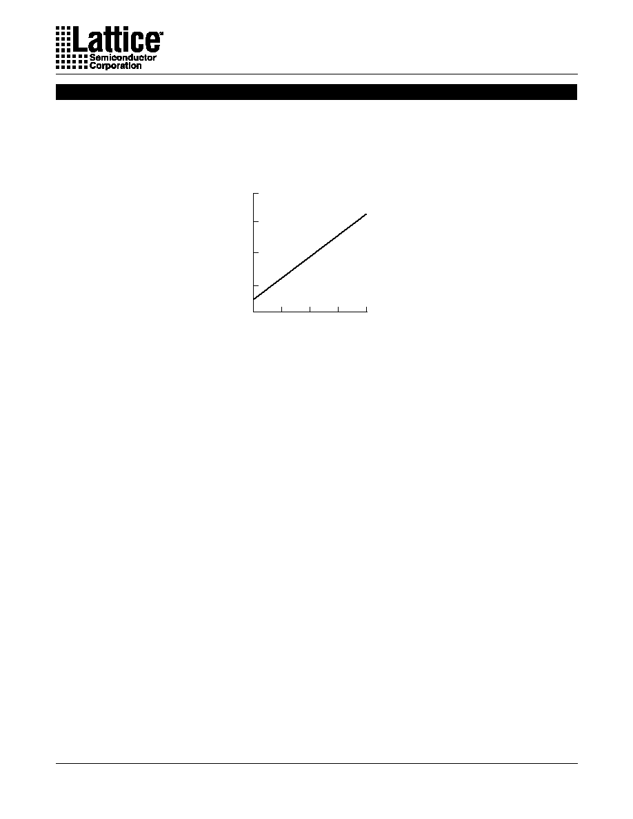
Power Consumption
Power consumption in the ispLSI 2064VE device de-
pends on two primary factors: the speed at which the
device is operating and the number of Product Terms
used. Figure 3 shows the relationship between power
and operating speed.
Figure 3. Typical Device Power Consumption vs fmax
0127/2064VE
ICC can be estimated for the ispLSI 2064VE using the following equation:
ICC(mA) = 8 + (# of PTs * 0.67) + (# of Nets * Max. Freq. * 0.0045)
Where:
# of PTs = Number of Product Terms used in design
# of nets = Number of Signals used in device
Max freq = Highest Clock Frequency to the device (in MHz)
The ICC estimate is based on typical conditions (VCC = 3.3V, room temperature) and an assumption of two GLB
loads on average exists. These values are for estimates only. Since the value of ICC is sensitive to operating
conditions and the program in the device, the actual ICC should be verified.
Notes: Configuration of four 16-bit counters
Typical current at 3.3V, 25
∞
C
100
140
0
50
100
150
200
f
max (MHz)
ispLSI 2064VE
160
120
80
I
CC (mA)
10
Specifications
ispLSI 2064VE
32-I/O Signal Descriptions
GOE 0/IN 3
This pin performs one of two functions. It can be programmed to function as a Global Output Enable
pin or a Dedicated Input pin.
GOE 1/Y0
This pin performs one of two functions. It can be programmed to function as a GLobal Output Enable or
a Dedicated Clock input. This clock input is connected to one of the clock inputs of all GLBs on the
device.
RESET
/Y1
This pin performs two functions: (1) Dedicated clock input. This clock input is brought into the Clock
Deistribution Network and can optionally be routed to any GLB and/or I/O cell on the device. (2) Active
Low (0) Reset pin which resets all of the registers in the device.
BSCAN
Input ≠ Dedicated in-system programming Boundary Scan Enable input pin. This pin is brought low to
enable the programming mode. The TMS, TDI, TDO and TCK controls become active.
TDI/IN 0
Input ≠ This pin performs two functions. When
BSCAN
is logic low, it functions as an input pin to load
programming data into the device. TDI/IN0 is also used as one of the two control pins for the ISP State
Machine. When
BSCAN
is high, it functions as a dedicated input pin.
TMS/IN 2
Input ≠ This pin performs two functions. When
BSCAN
is logic low, it functions as a pin to control the
operation of the ISP State Machine. When
BSCAN
is high, it functions as a dedicated input pin.
TDO/IN 1
Output/Input ≠ This pin performs two functions. When
BSCAN
is logic low, it functions as an output pin
pin to read serial shift register data. When
BSCAN
is high, it functions as a dedicated input pin.
TCK/Y2
Input ≠ This pin performs two functions. When
BSCAN
is logic low, it functions as a clock pin for the
Serial Shift Register. When
BSCAN
is high, it functions as a dedicated clock input. This clock input is
brought into the Clock Distribution Network and can optionally be routed to any GLB and/or I/O cell on
the device.
GND
Ground (GND)
VCC
Vcc
NC
1
No Connect
I/O
Input/Output pins ≠ These are the general purpose I/O pins used by the logic array.
64-I/O Signal Descriptions
RESET
Active Low (0) Reset pin resets all the registers in the device.
GOE 0, GOE1
Global Output Enable input pins.
Y0, Y1, Y2
Dedicated Clock Input ≠ These clock inputs are connected to one of the clock inputs of all the GLBs in
the device.
BSCAN
Input ≠ Dedicated in-system programming Boundary Scan enable input pin. This pin is brought low to
enable the programming mode. The TMS, TDI, TDO and TCK controls become active.
TDI/IN 0
Input ≠ This pin performs two functions. When
BSCAN
is logic low, it functions as an input pin to load
programming data into the device. TDI/IN0 is also used as one of the two control pins for the ISP State
Machine. When
BSCAN
is high, it functions as a dedicated input pin.
TCK/IN 3
Input ≠ This pin performs two functions. When
BSCAN
is logic low, it functions as a clock pin for the
Boundary Scan state machine. When
BSCAN
is high, it functions as a dedicated input pin.
TMS/IN 1
Input ≠ This pin performs two functions. When
BSCAN
is logic low, it functions as a mode control pin for
the Boundary Scan state machine. When
BSCAN
is high, it functions as a dedicated input pin.
TDO/IN 2
Output/Input ≠ This pin performs two functions. When
BSCAN
is logic low, it functions as an output pin
to read serial shift register data. When
BSCAN
is high, it functions as a dedicated input pin.
GND
Ground (GND)
VCC
Vcc
NC
1
No Connect
I/O
Input/Output Pins ≠ These are the general purpose I/O pins used by the logic array.
Signal Name Description
1. NC pins are not to be connected to any active signals, VCC or GND.
Signal Name Description
1. NC pins are not to be connected to any active signals, VCC or GND.
11
Specifications
ispLSI 2064VE
64-I/O Signal Locations
32-I/O Signal Locations
l
a
n
g
i
S
A
G
B
a
c
l
l
a
B
-
0
0
1
P
F
Q
T
n
i
P
-
0
0
1
T
E
S
E
R
2
D
1
1
1
E
O
G
,
0
E
O
G
1
E
,
9
F
3
1
,
2
6
2
Y
,
1
Y
,
0
Y
8
F
,
6
F
,
3
E
0
6
,
5
6
,
0
1
N
A
C
S
B
5
E
5
1
0
N
I
/
I
D
T
2
F
6
1
3
N
I
/
K
C
T
0
1
G
9
5
1
N
I
/
S
M
T
5
J
7
3
2
N
I
/
O
D
T
6
B
7
8
D
N
G
6
K
,
9
G
,
1
F
,
7
B
6
8
,
1
6
,
9
3
,
4
1
C
C
V
4
J
,
0
1
F
,
2
E
,
5
A
9
8
,
3
6
,
6
3
,
2
1
C
N
1
,
4
C
,
3
C
,
8
A
,
6
A
,
7
E
,
8
D
,
6
D
,
1
D
,
4
F
,
0
1
E
,
9
E
,
8
H
,
7
H
,
5
G
,
3
G
5
K
,
3
K
,
5
2
,
1
2
,
9
,
4
,
0
5
,
4
4
,
8
3
,
1
3
,
1
7
,
6
6
,
4
6
,
4
5
,
4
9
,
8
8
,
1
8
,
5
7
0
0
1
,
s
l
a
n
g
i
s
e
v
i
t
c
a
y
n
a
o
t
d
e
t
c
e
n
n
o
c
e
b
o
t
t
o
n
e
r
a
s
n
i
p
C
N
.
1
.
D
N
G
r
o
C
C
V
l
a
n
g
i
S
P
F
Q
T
n
i
P
-
4
4
C
C
L
P
n
i
P
-
4
4
3
N
I
/
0
E
O
G
0
4
2
0
Y
/
1
E
O
G
5
1
1
T
E
S
E
R
1
Y
/
9
2
5
3
N
A
C
S
B
7
3
1
0
N
I
/
I
D
T
8
4
1
2
N
I
/
S
M
T
0
3
6
3
1
N
I
/
O
D
T
8
1
4
2
2
Y
/
K
C
T
7
2
3
3
D
N
G
9
3
,
7
1
3
2
,
1
C
C
V
8
2
,
6
4
3
,
2
1
C
N
1
--
--
,
s
l
a
n
g
i
s
e
v
i
t
c
a
y
n
a
o
t
d
e
t
c
e
n
n
o
c
e
b
o
t
t
o
n
e
r
a
s
n
i
p
C
N
.
1
.
D
N
G
r
o
C
C
V
I/O Locations
I/O 0
G1
17
9
15
I/O 1
F3
18
10
16
I/O 2
E4
19
11
17
I/O 3
H1
20
12
18
I/O 4
G2
22
13
19
I/O 5
J1
23
14
20
I/O 6
H2
24
15
21
I/O 7
K1
26
16
22
I/O 8
J2
27
19
25
I/O 9
K2
28
20
26
I/O 10
H3
29
21
27
I/O 11
J3
30
22
28
I/O 12
G4
32
23
29
I/O 13
H4
33
24
30
I/O 14
K4
34
25
31
I/O 15
H5
35
26
32
I/O 16
F5
40
31
37
I/O 17
J6
41
32
38
I/O 18
K7
42
33
39
I/O 19
H6
43
34
40
I/O 20
K8
45
35
41
I/O 21
G6
46
36
42
I/O 22
J7
47
37
43
I/O 23
K9
48
38
44
I/O 24
J8
49
41
3
I/O 25
K10
51
42
4
I/O 26
J9
52
43
5
I/O 27
J10
53
44
6
I/O 28
H9
55
1
7
I/O 29
H10
56
2
8
I/O 30
G7
57
3
9
I/O 31
G8
58
4
10
I/O 32
D10
67
--
--
I/O 33
E8
68
--
--
I/O 34
F7
69
--
--
I/O 35
C10
70
--
--
I/O 36
D9
72
--
--
I/O 37
B10
73
--
--
I/O 38
C9
74
--
--
I/O 39
A10
76
--
--
I/O 40
B9
77
--
--
I/O 41
A9
78
--
--
I/O 42
C8
79
--
--
I/O 43
B8
80
--
--
I/O 44
D7
82
--
--
I/O 45
C7
83
--
--
I/O 46
A7
84
--
--
I/O 47
C6
85
--
--
I/O 48
E6
90
--
--
I/O 49
B5
91
--
--
I/O 50
A4
92
--
--
I/O 51
C5
93
--
--
I/O 52
A3
95
--
--
I/O 53
D5
96
--
--
I/O 54
B4
97
--
--
I/O 55
A2
98
--
--
I/O 56
B3
99
--
--
I/O 57
A1
1
--
--
I/O 58
B2
2
--
--
I/O 59
B1
3
--
--
I/O 60
C2
5
--
--
I/O 61
C1
6
--
--
I/O 62
D4
7
--
--
I/O 63
D3
8
--
--
100
100
44
44
Signal
caBGA
TQFP
TQFP
PLCC
12
Specifications
ispLSI 2064VE
Signal Configuration
ispLSI 2064VE 100-Ball caBGA Signal Diagram
10
9
8
7
6
5
4
3
2
1
A
B
C
D
E
F
G
H
J
K
A
B
C
D
E
F
G
H
J
K
10
9
8
7
6
5
4
3
2
1
I/O
39
I/O
41
I/O
46
I/O
50
I/O
52
I/O
55
I/O
57
NC
1
NC
1
VCC
I/O
35
I/O
38
I/O
42
I/O
45
I/O
47
I/O
51
I/O
60
I/O
61
NC
1
NC
1
TCK/
IN 3
I/O
31
I/O
30
I/O
21
I/O
12
I/O
4
I/O
0
NC
1
GND
NC
1
I/O
29
I/O
28
I/O
19
I/O
13
I/O
10
I/O
15
I/O
6
I/O
3
NC
1
NC
1
I/O
27
I/O
26
I/O
24
I/O
22
I/O
17
I/O
11
TMS/
IN 1
I/O
8
I/O
5
VCC
I/O
25
1
NCs are not to be connected to any active signals, VCC or GND.
Note: Ball A1 indicator dot on top side of package.
I/O
23
I/O
20
I/O
18
I/O
14
I/O
9
I/O
7
GND
NC
1
NC
1
GOE
0
I/O
34
I/O
16
I/O
1
TDI/
IN 0
NC
1
GND
100-BGA/2064VE
VCC
Y2
Y1
I/O
32
I/O
36
I/O
44
I/O
53
I/O
62
I/O
63
NC
1
NC
1
NC
1
RESET
I/O
33
I/O
48
I/O
2
GOE
1
NC
1
VCC
Y0
NC
1
NC
1
BSCAN
I/O
37
I/O
40
I/O
43
I/O
54
I/O
49
TDO/
IN 2
I/O
56
I/O
58
I/O
59
GND
ispLSI 2064VE
Bottom View
13
Specifications
ispLSI 2064VE
Pin Configuration
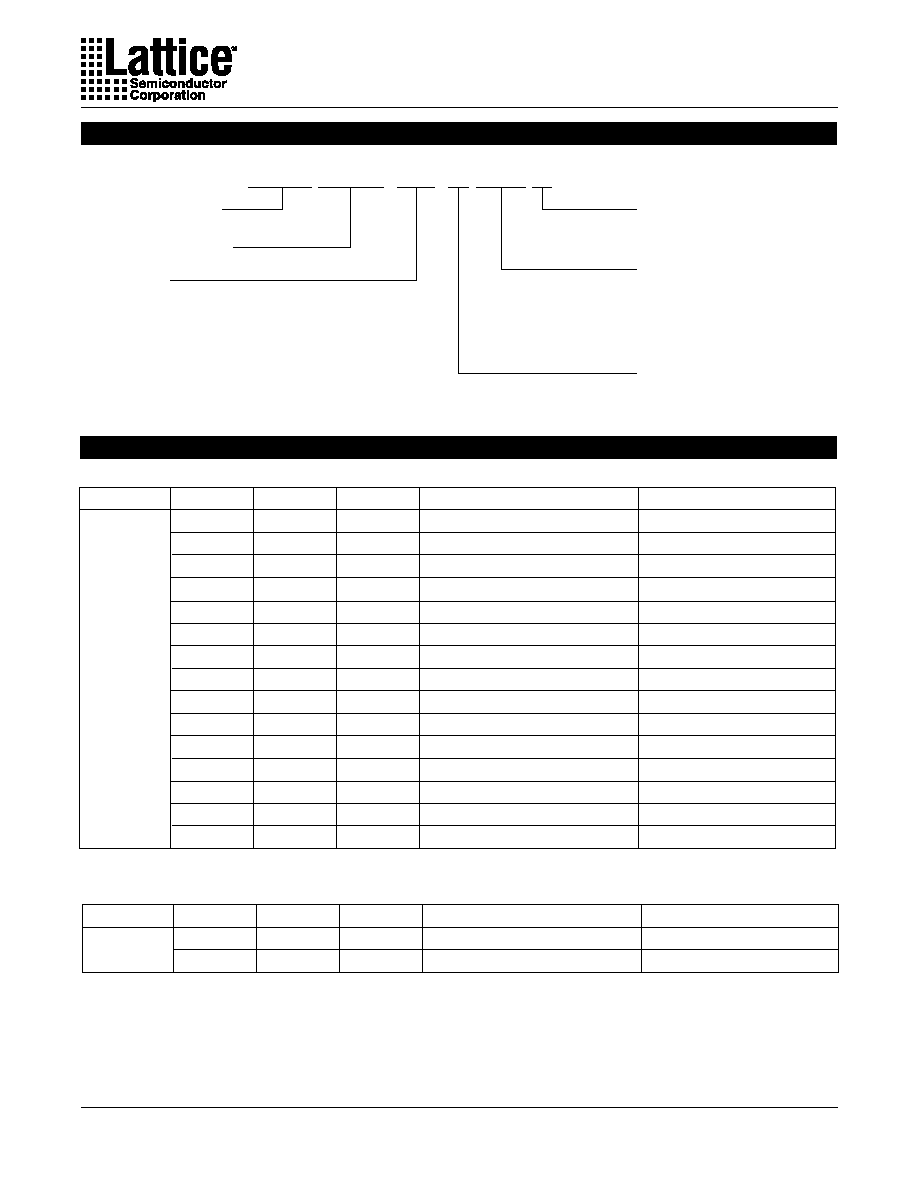
ispLSI 2064VE 100-Pin TQFP Pinout Diagram
I/O 57
I/O 58
I/O 59
1
NC
I/O 60
I/O 61
I/O 62
I/O 63
1
NC
Y0
RESET
VCC
GOE 1
GND
BSCAN
TDI/IN 0
I/O 0
I/O 1
I/O 2
I/O 3
1
NC
I/O 4
I/O 5
I/O 6
1
NC
NC
1
I/O 38
I/O 37
I/O 36
NC
1
I/O 35
I/O 34
I/O 33
I/O 32
NC
1
Y1
NC
1
VCC
GOE 0
GND
Y2
TCK/IN 3
I/O 31
I/O 30
I/O 29
I/O 28
NC
1
I/O 27
I/O 26
I/O 25
NC
1
I/O 56
I/O 55
I/O 54
I/O 53
I/O 52
NC
1
I/O 51
I/O 50
I/O 49
I/O 48
VCC
NC
1
TDO/IN 2
GND
I/O 47
I/O 46
I/O 45
I/O 44
NC
1
I/O 43
I/O 42
I/O 41
I/O 40
I/O 39
I/O 7
I/O 8
I/O 9
I/O 10
I/O 11
1
NC
I/O 12
I/O 13
I/O 14
I/O 15
VCC
TMS/IN 1
1
NC
GND
I/O 16
I/O 17
I/O 18
I/O 19
1
NC
I/O 20
I/O 21
I/O 22
I/O 23
I/O 24
1
NC
1
2
3
4
5
6
7
8
9
10
11
12
13
14
15
16
17
18
19
20
21
22
23
24
25
75
74
73
72
71
70
69
68
67
66
65
64
63
62
61
60
59
57
56
55
54
53
52
51
26
27
28
29
30
31
32
33
34
35
36
37
38
39
40
41
42
43
44
45
46
47
48
49
50
100
99
98
97
96
95
94
93
92
91
90
89
88
87
86
85
84
83
82
81
80
79
78
77
76
58
ispLSI 2064VE
Top View
1. NC pins are not to be connected to any active signals, VCC or GND.
100 TQFP/2064VE
14
Specifications
ispLSI 2064VE
Pin Configuration
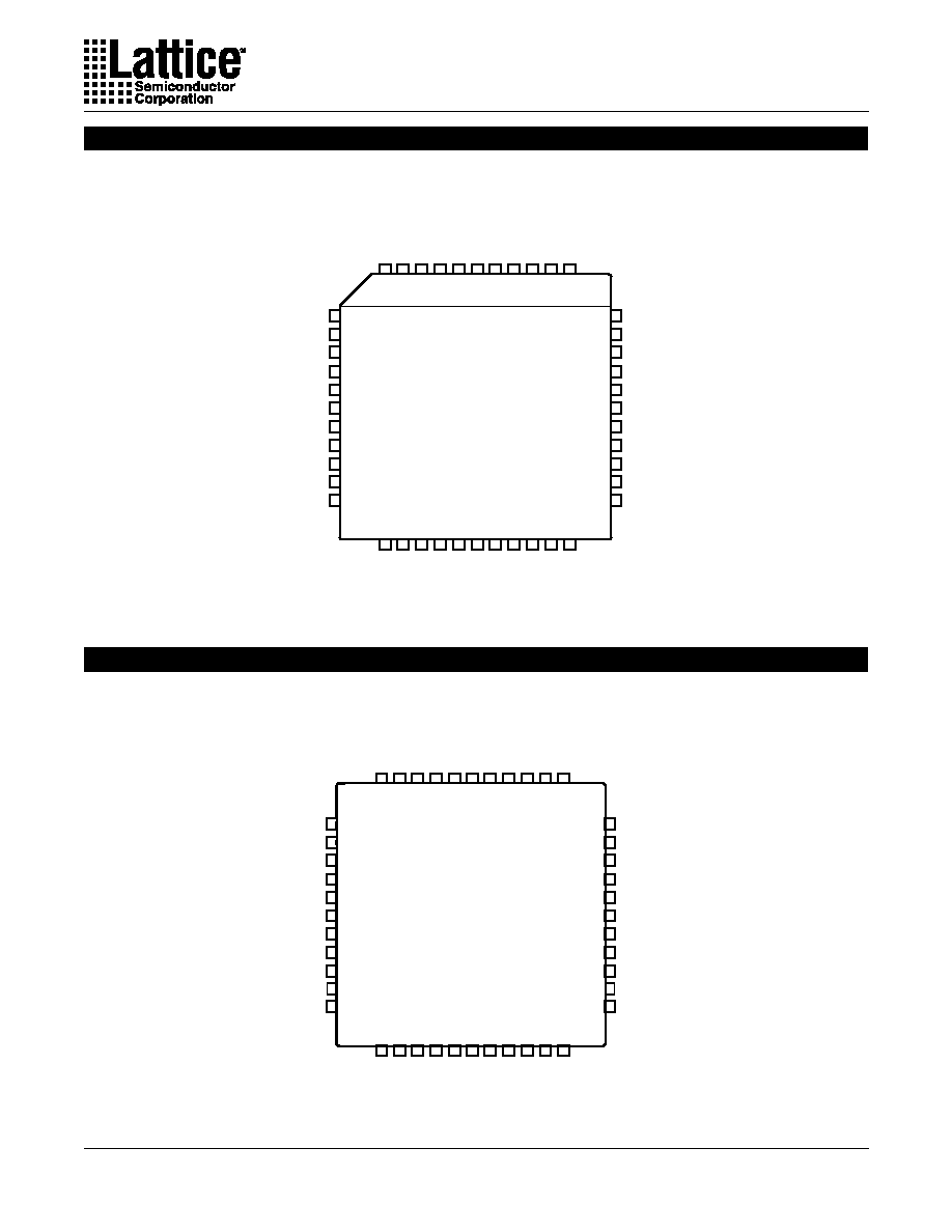
ispLSI 2064VE 44-Pin PLCC Pinout Diagram
I/O 18
I/O 17
I/O 16
TMS/IN 2
RESET
/Y1
VCC
TCK/Y2
I/O 15
I/O 14
I/O 13
I/O 12
I/O 28
I/O 29
I/O 30
I/O 31
GOE1/Y0
VCC
BSCAN
TDI/IN 0
I/O 0
I/O 1
I/O 2
I/O 27
I/O 26
I/O 25
I/O 24
GOE 0/IN 3
GND
I/O 23
I/O 22
I/O 21
I/O 20
I/O 19
I/O 3
I/O 4
I/O 5
I/O 6
I/O 7
GND
TDO/IN 1
I/O 8
I/O 9
I/O 10
I/O 11
ispLSI 2064VE
Top View
1
2
3
4
6
5
7
8
9
10
11
33
32
31
30
29
28
27
26
25
24
23
44
12
43
13
42
14
41
15
40
16
39
17
38
18
37
19
36
20
35
21
34
22
44 TQFP/2064VE
I/O 18
I/O 17
I/O 16
TMS/IN 2
RESET
/Y1
VCC
TCK/Y2
I/O 15
I/O 14
I/O 13
I/O 12
I/O 28
I/O 29
I/O 30
I/O 31
GOE1/Y0
VCC
BSCAN
TDI/IN 0
I/O 0
I/O 1
I/O 2
I/O 27
I/O 26
I/O 25
I/O 24
GOE 0/IN 3
GND
I/O 23
I/O 22
I/O 21
I/O 20
I/O 19
I/O 3
I/O 4
I/O 5
I/O 6
I/O 7
GND
TDO/IN 1
I/O 8
I/O 9
I/O 10
I/O 11
ispLSI 2064VE
Top View
7
8
9
10
12
11
13
14
15
16
17
39
38
37
36
35
34
33
32
31
30
29
6
18
5
19
4
20
3
21
2
22
1
23
44
24
43
25
42
26
41
27
40
28
44 PLCC/2064VE
Pin Configuration
ispLSI 2064VE 44-Pin TQFP Pinout Diagram
15
Specifications
ispLSI 2064VE
Part Number Description
ispLSI 2064VE Ordering Information
135
7.5
100-Pin TQFP
ispLSI 2064VE-135LT100
Table 2-0041A/2064VE
135
100-Ball caBGA
7.5
ispLSI 2064VE-135LB100
FAMILY
fmax (MHz)
200
ORDERING NUMBER
PACKAGE
100-Pin TQFP
tpd (ns)
4.5
ispLSI
ispLSI 2064VE-200LT100
64
64
135
7.5
44-Pin PLCC
ispLSI 2064VE-135LJ44
135
44-Pin TQFP
7.5
ispLSI 2064VE-135LT44
32
32
I/Os
64
200
100-Ball caBGA
4.5
ispLSI 2064VE-200LB100
64
280
100-Pin TQFP
3.5
ispLSI 2064VE-280LT100*
64
280
100-Ball caBGA
3.5
ispLSI 2064VE-280LB100*
64
200
44-Pin PLCC
4.5
ispLSI 2064VE-200LJ44
32
200
44-Pin TQFP
4.5
ispLSI 2064VE-200LT44
32
280
44-Pin TQFP
3.5
ispLSI 2064VE-280LT44*
32
100
100
100-Pin TQFP
10
10
ispLSI 2064VE-100LT100
100-Ball caBGA
ispLSI 2064VE-100LB100
64
64
100
100
44-Pin PLCC
10
10
ispLSI 2064VE-100LJ44
44-Pin TQFP
ispLSI 2064VE-100LT44
*Advanced Information
32
32
COMMERCIAL
Table 2-0041B/2064VE
ispLSI
135
7.5
100-Pin TQFP
ispLSI 2064VE-135LT100I
64
135
7.5
44-Pin TQFP
ispLSI 2064VE-135LT44I
32
INDUSTRIAL
FAMILY
fmax (MHz)
ORDERING NUMBER
PACKAGE
tpd (ns)
I/Os
Device Number
ispLSI 2064VE XXX X XXXX
Grade
Blank = Commercial
I = Industrial
X
Speed
280 = 280 MHz
f
max*
200 = 200 MHz
f
max
135 = 135 MHz
f
max
100 = 100 MHz
f
max
*Advanced Information
Power
L = Low
Package
T100 = 100-Pin TQFP
B100 = 100-Ball caBGA
T44 = 44-Pin TQFP
J44 = 44-Pin PLCC
≠
Device Family
0212/2064VE