Specifications
GAL16V8
1996 Data Book
3-65
1
10
11
20
I/CLK
I
I
I
I
I
I
I
I
GND
Vcc
I/O/Q
I/O/Q
I/O/Q
I/O/Q
I/O/Q
I/O/Q
I/O/Q
I/O/Q
I/OE
5
15
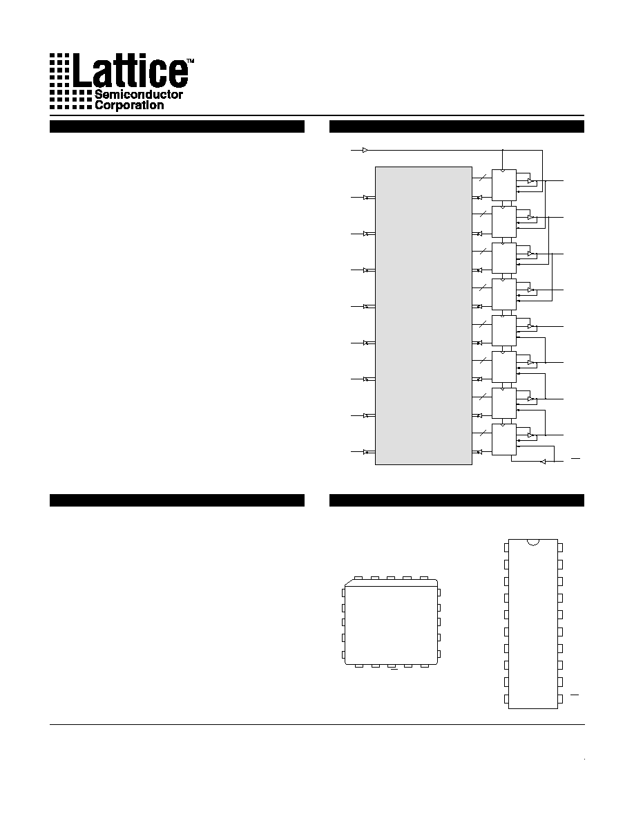
FUNCTIONAL BLOCK DIAGRAM
FEATURES
PIN CONFIGURATION
� HIGH PERFORMANCE E
2
CMOS
�
TECHNOLOGY
-- 5 ns Maximum Propagation Delay
-- Fmax = 166 MHz
-- 4 ns Maximum from Clock Input to Data Output
-- UltraMOS
�
Advanced CMOS Technology
� 50% to 75% REDUCTION IN POWER FROM BIPOLAR
-- 75mA Typ Icc on Low Power Device
-- 45mA Typ Icc on Quarter Power Device
� ACTIVE PULL-UPS ON ALL PINS
� E
2
CELL TECHNOLOGY
-- Reconfigurable Logic
-- Reprogrammable Cells
-- 100% Tested/Guaranteed 100% Yields
-- High Speed Electrical Erasure (<100ms)
-- 20 Year Data Retention
� EIGHT OUTPUT LOGIC MACROCELLS
-- Maximum Flexibility for Complex Logic Designs
-- Programmable Output Polarity
-- Also Emulates 20-pin PAL
�
Devices with Full Func-
tion/Fuse Map/Parametric Compatibility
� PRELOAD AND POWER-ON RESET OF ALL REGISTERS
-- 100% Functional Testability
� APPLICATIONS INCLUDE:
-- DMA Control
-- State Machine Control
-- High Speed Graphics Processing
-- Standard Logic Speed Upgrade
� ELECTRONIC SIGNATURE FOR IDENTIFICATION
DESCRIPTION
The GAL16V8C, at 5 ns maximum propagation delay time, com-
bines a high performance CMOS process with Electrically Eras-
able (E
2
) floating gate technology to provide the highest speed
performance available in the PLD market. High speed erase times
(<100ms) allow the devices to be reprogrammed quickly and ef-
ficiently.
The generic architecture provides maximum design flexibility by
allowing the Output Logic Macrocell (OLMC) to be configured by
the user. An important subset of the many architecture configu-
rations possible with the GAL16V8 are the PAL
architectures
listed in the table of the macrocell description section. GAL16V8
devices are capable of emulating any of these PAL architectures
with full function/fuse map/parametric compatibility.
Unique test circuitry and reprogrammable cells allow complete
AC, DC, and functional testing during manufacture. As a result,
Lattice Semiconductor guarantees 100% field programmability
and functionality of all GAL products. In addition, 100 erase/write
cycles and data retention in excess of 20 years are guaranteed.
PLCC
GAL
16V8
DIP
GAL16V8
Top View
2
20
I/CLK
I
I
I
I
I
I
I
I
GND
Vcc
I/O/Q
I/O/Q
I/O/Q
I/O/Q
I/O/Q
I/O/Q
I/O/Q
I/O/Q
I/OE
4
6
8
9
11
13
14
16
18
I/CLK
I
I/O/Q
I
I/O/Q
I
I/O/Q
I
I/O/Q
I
I/O/Q
I
I/O/Q
I
I/O/Q
I
I/O/Q
CLK
8
8
8
8
8
8
8
8
OE
OLMC
OLMC
OLMC
OLMC
OLMC
OLMC
OLMC
OLMC
PROGRAMMABLE
AND-ARRAY
(64 X 32)
I/OE
GAL16V8
High Performance E
2
CMOS PLD
Generic Array LogicTM
Copyright � 1996 Lattice Semiconductor Corporation. E2CMOS, GAL, ispGAL, ispLSI, pLSI, pDS, Silicon Forest, UltraMOS, L with Lattice Semiconductor Corp. and L (Stylized) are registered
trademarks of Lattice Semiconductor Corporation (LSC). The LSC Logo, Generic Array Logic, In-System Programmability, In-System Programmable, ISP, ispATE, ispCODE, ispDOWNLOAD,
ispGDS, ispStarter, ispSTREAM, ispTEST, ispTURBO, Latch-Lock, pDS+, RFT, Total ISP and Twin GLB are trademarks of Lattice Semiconductor Corporation. ISP is a service mark of Lattice
Semiconductor Corporation. All brand names or product names mentioned are trademarks or registered trademarks of their respective holders.
LATTICE SEMICONDUCTOR CORP., 5555 Northeast Moore Ct., Hillsboro, Oregon 97124, U.S.A.
1996 Data Book
Tel. (503) 681-0118; 1-888-ISP-PLDS; FAX (503) 681-3037; http://www.lattice.com

Specifications
GAL16V8
1996 Data Book
3-67
OUTPUT LOGIC MACROCELL (OLMC)
The following discussion pertains to configuring the output logic
macrocell. It should be noted that actual implementation is ac-
complished by development software/hardware and is completely
transparent to the user.
There are three global OLMC configuration modes possible:
simple, complex, and registered. Details of each of these
modes are illustrated in the following pages. Two global bits, SYN
and AC0, control the mode configuration for all macrocells. The
XOR bit of each macrocell controls the polarity of the output in any
of the three modes, while the AC1 bit of each of the macrocells
controls the input/output configuration. These two global and 16
individual architecture bits define all possible configurations in a
GAL16V8 . The information given on these architecture bits is
only to give a better understanding of the device. Compiler soft-
ware will transparently set these architecture bits from the pin
definitions, so the user should not need to directly manipulate
these architecture bits.
The following is a list of the PAL architectures that the GAL16V8
can emulate. It also shows the OLMC mode under which the
GAL16V8 emulates the PAL architecture.
PAL Architectures
GAL16V8
Emulated by GAL16V8
Global OLMC Mode
16R8
Registered
16R6
Registered
16R4
Registered
16RP8
Registered
16RP6
Registered
16RP4
Registered
16L8
Complex
16H8
Complex
16P8
Complex
10L8
Simple
12L6
Simple
14L4
Simple
16L2
Simple
10H8
Simple
12H6
Simple
14H4
Simple
16H2
Simple
10P8
Simple
12P6
Simple
14P4
Simple
16P2
Simple
COMPILER SUPPORT FOR OLMC
Software compilers support the three different global OLMC
modes as different device types. These device types are listed
in the table below. Most compilers have the ability to automati-
cally select the device type, generally based on the register usage
and output enable (OE) usage. Register usage on the device
forces the software to choose the registered mode. All combina-
torial outputs with OE controlled by the product term will force the
software to choose the complex mode. The software will choose
the simple mode only when all outputs are dedicated combinatorial
without OE control. The different device types listed in the table
can be used to override the automatic device selection by the
software. For further details, refer to the compiler software
manuals.
When using compiler software to configure the device, the user
must pay special attention to the following restrictions in each
mode.
In registered mode pin 1 and pin 11 are permanently configured
as clock and output enable, respectively. These pins cannot be
configured as dedicated inputs in the registered mode.
In complex mode pin 1 and pin 11 become dedicated inputs and
use the feedback paths of pin 19 and pin 12 respectively. Because
of this feedback path usage, pin 19 and pin 12 do not have the
feedback option in this mode.
In simple mode all feedback paths of the output pins are routed
via the adjacent pins. In doing so, the two inner most pins ( pins
15 and 16) will not have the feedback option as these pins are
always configured as dedicated combinatorial output.
Registered
Complex
Simple
Auto Mode Select
ABEL
P16V8R
P16V8C
P16V8AS
P16V8
CUPL
G16V8MS
G16V8MA
G16V8AS
G16V8
LOG/iC
GAL16V8_R
GAL16V8_C7
GAL16V8_C8
GAL16V8
OrCAD-PLD
"Registered"
1
"Complex"
1
"Simple"
1
GAL16V8A
PLDesigner
P16V8R
2
P16V8C
2
P16V8C
2
P16V8A
TANGO-PLD
G16V8R
G16V8C
G16V8AS
3
G16V8
1) Used with Configuration keyword.
2) Prior to Version 2.0 support.
3) Supported on Version 1.20 or later.

Specifications
GAL16V8
1996 Data Book
3-68
REGISTERED MODE
In the Registered mode, macrocells are configured as dedicated
registered outputs or as I/O functions.
Architecture configurations available in this mode are similar to
the common 16R8 and 16RP4 devices with various permutations
of polarity, I/O and register placement.
All registered macrocells share common clock and output enable
control pins. Any macrocell can be configured as registered or
I/O. Up to eight registers or up to eight I/O's are possible in this
mode. Dedicated input or output functions can be implemented
as subsets of the I/O function.
Registered outputs have eight product terms per output. I/O's
have seven product terms per output.
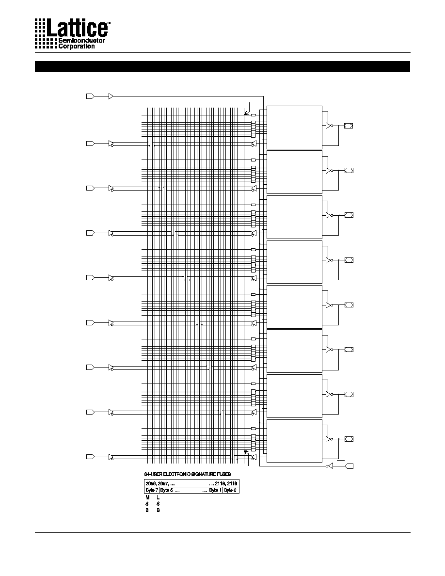
The JEDEC fuse numbers, including the User Electronic Signature
(UES) fuses and the Product Term Disable (PTD) fuses, are
shown on the logic diagram on the following page.
Registered Configuration for Registered Mode
- SYN=0.
- AC0=1.
- XOR=0 defines Active Low Output.
- XOR=1 defines Active High Output.
- AC1=0 defines this output configuration.
- Pin 1 controls common CLK for the registered outputs.
- Pin 11 controls common OE for the registered outputs.
- Pin 1 & Pin 11 are permanently configured as CLK &
OE.
Combinatorial Configuration for Registered Mode
- SYN=0.
- AC0=1.
- XOR=0 defines Active Low Output.
- XOR=1 defines Active High Output.
- AC1=1 defines this output configuration.
- Pin 1 & Pin 11 are permanently configured as CLK &
OE.
Note: The development software configures all of the architecture control bits and checks for proper pin usage automatically.
D
Q
Q
CLK
OE
XOR
XOR