
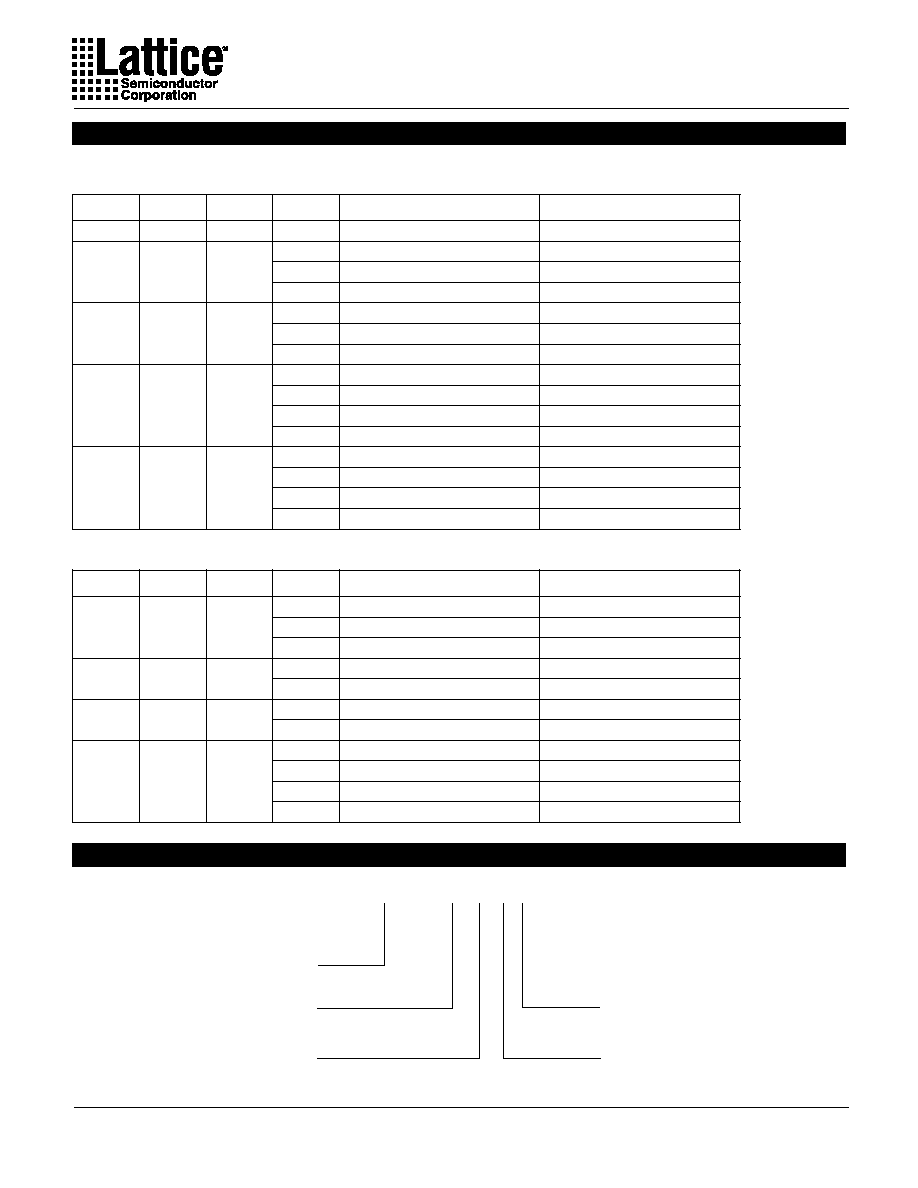
GAL20V8
High Performance E
2
CMOS PLD
Generic Array LogicTM
1
2
28
NC
I/CLK
I
I
I
I
I
I
I
NC
NC
NC
GND
I
I
I/OE
I
I/O/Q
I/O/Q
I/O/Q
I/O/Q
I/O/Q
I/O/Q
I/O/Q
Vcc
I/O/Q
I
I
4
5
7
9
11
12
14
16
18
19
21
23
25
26
PLCC
1
12
13
24
I/CLK
I
I
I
I
I
I
I
I
I
I
GND
Vcc
I
I/O/Q
I/O/Q
I/O/Q
I/O/Q
I/O/Q
I/O/Q
I/O/Q
I/O/Q
I
I/OE
6
18
GAL20V8
Top View
GAL
20V8
DIP
CLK
I
I
I/O/Q
I/O/Q
I/O/Q
I/O/Q
I/O/Q
I/O/Q
I/O/Q
I/O/Q
I
I
I
I
I
I
I
I
I
I
I/OE
I/CLK
OE
8
8
8
8
8
8
8
8
OLMC
OLMC
OLMC
OLMC
OLMC
OLMC
OLMC
IMUX
IMUX
PROGRAMMABLE
AND-ARRAY
(64 X 40)
OLMC
Copyright � 2000 Lattice Semiconductor Corp. All brand or product names are trademarks or registered trademarks of their respective holders. The specifications and information herein are subject
to change without notice.
LATTICE SEMICONDUCTOR CORP., 5555 Northeast Moore Ct., Hillsboro, Oregon 97124, U.S.A.
August 2000
Tel. (503) 268-8000; 1-800-LATTICE; FAX (503) 268-8556; http://www.latticesemi.com
20v8_04
Features
� HIGH PERFORMANCE E
2
CMOS
�
TECHNOLOGY
-- 5 ns Maximum Propagation Delay
-- Fmax = 166 MHz
-- 4 ns Maximum from Clock Input to Data Output
-- UltraMOS
�
Advanced CMOS Technology
� 50% to 75% REDUCTION IN POWER FROM BIPOLAR
-- 75mA Typ Icc on Low Power Device
-- 45mA Typ Icc on Quarter Power Device
� ACTIVE PULL-UPS ON ALL PINS
� E
2
CELL TECHNOLOGY
-- Reconfigurable Logic
-- Reprogrammable Cells
-- 100% Tested/100% Yields
-- High Speed Electrical Erasure (<100ms)
-- 20 Year Data Retention
� EIGHT OUTPUT LOGIC MACROCELLS
-- Maximum Flexibility for Complex Logic Designs
-- Programmable Output Polarity
-- Also Emulates 24-pin PAL
�
Devices with Full Function/
Fuse Map/Parametric Compatibility
� PRELOAD AND POWER-ON RESET OF ALL REGISTERS
-- 100% Functional Testability
� APPLICATIONS INCLUDE:
-- DMA Control
-- State Machine Control
-- High Speed Graphics Processing
-- Standard Logic Speed Upgrade
� ELECTRONIC SIGNATURE FOR IDENTIFICATION
Description
The GAL20V8C, at 5ns maximum propagation delay time, com-
bines a high performance CMOS process with Electrically Eras-
able (E
2
) floating gate technology to provide the highest speed
performance available in the PLD market. High speed erase times
(<100ms) allow the devices to be reprogrammed quickly and ef-
ficiently.
The generic architecture provides maximum design flexibility by
allowing the Output Logic Macrocell (OLMC) to be configured by
the user. An important subset of the many architecture configura-
tions possible with the GAL20V8 are the PAL
architectures listed
in the table of the macrocell description section. GAL20V8 devices
are capable of emulating any of these PAL architectures with full
function/fuse map/parametric compatibility.
Unique test circuitry and reprogrammable cells allow complete AC,
DC, and functional testing during manufacture. As a result, Lattice
Semiconductor delivers 100% field programmability and function-
ality of all GAL products. In addition, 100 erase/write cycles and
data retention in excess of 20 years are specified.
Functional Block Diagram
Pin Configuration
2
Specifications
GAL20V8
)
s
n
(
d
p
T
)
s
n
(
u
s
T
)
s
n
(
o
c
T
)
A
m
(
c
c
I
#
g
n
i
r
e
d
r
O
e
g
a
k
c
a
P
0
1
0
1
7
0
3
1
8
V
0
2
L
A
G
C
I
J
L
0
1
-
C
C
L
P
d
a
e
L
-
8
2
0
3
1
I
P
L
0
1
-
B
8
V
0
2
L
A
G
P
I
D
c
i
t
s
a
l
P
n
i
P
-
4
2
0
3
1
I
J
L
0
1
-
B
8
V
0
2
L
A
G
C
C
L
P
d
a
e
L
-
8
2
5
1
2
1
0
1
0
3
1
I
P
L
5
1
-
B
8
V
0
2
L
A
G
P
I
D
c
i
t
s
a
l
P
n
i
P
-
4
2
0
3
1
I
J
L
5
1
-
B
8
V
0
2
L
A
G
C
C
L
P
d
a
e
L
-
8
2
0
2
3
1
1
1
5
6
I
P
Q
0
2
-
B
8
V
0
2
L
A
G
P
I
D
c
i
t
s
a
l
P
n
i
P
-
4
2
5
6
I
J
Q
0
2
-
B
8
V
0
2
L
A
G
C
C
L
P
d
a
e
L
-
8
2
5
2
5
1
2
1
5
6
I
P
Q
5
2
-
B
8
V
0
2
L
A
G
P
I
D
c
i
t
s
a
l
P
n
i
P
-
4
2
5
6
I
J
Q
5
2
-
B
8
V
0
2
L
A
G
C
C
L
P
d
a
e
L
-
8
2
0
3
1
I
P
L
5
2
-
B
8
V
0
2
L
A
G
P
I
D
c
i
t
s
a
l
P
n
i
P
-
4
2
0
3
1
I
J
L
5
2
-
B
8
V
0
2
L
A
G
C
C
L
P
d
a
e
L
-
8
2
Industrial Grade Specifications
Blank = Commercial
I = Industrial
Grade
Package
Power
L = Low Power
Q = Quarter Power
Speed (ns)
XXXXXXXX
XX
X
X X
Device Name
_
P = Plastic DIP
J = PLCC
GAL20V8C
GAL20V8B
)
s
n
(
d
p
T
)
s
n
(
u
s
T
)
s
n
(
o
c
T
)
A
m
(
c
c
I
#
g
n
i
r
e
d
r
O
e
g
a
k
c
a
P
5
3
4
5
1
1
J
L
5
-
C
8
V
0
2
L
A
G
C
C
L
P
d
a
e
L
-
8
2
5
.
7
7
5
5
1
1
8
V
0
2
L
A
G
C
J
L
7
-
C
C
L
P
d
a
e
L
-
8
2
5
1
1
P
L
7
-
B
8
V
0
2
L
A
G
P
I
D
c
i
t
s
a
l
P
n
i
P
-
4
2
5
1
1
J
L
7
-
B
8
V
0
2
L
A
G
C
C
L
P
d
a
e
L
-
8
2
0
1
0
1
7
5
1
1
8
V
0
2
L
A
G
C
J
L
0
1
-
C
C
L
P
d
a
e
L
-
8
2
5
1
1
P
L
0
1
-
B
8
V
0
2
L
A
G
P
I
D
c
i
t
s
a
l
P
n
i
P
-
4
2
5
1
1
J
L
0
1
-
B
8
V
0
2
L
A
G
C
C
L
P
d
a
e
L
-
8
2
5
1
2
1
0
1
5
5
P
Q
5
1
-
B
8
V
0
2
L
A
G
P
I
D
c
i
t
s
a
l
P
n
i
P
-
4
2
5
5
J
Q
5
1
-
B
8
V
0
2
L
A
G
C
C
L
P
d
a
e
L
-
8
2
0
9
P
L
5
1
-
B
8
V
0
2
L
A
G
P
I
D
c
i
t
s
a
l
P
n
i
P
-
4
2
0
9
J
L
5
1
-
B
8
V
0
2
L
A
G
C
C
L
P
d
a
e
L
-
8
2
5
2
5
1
2
1
5
5
P
Q
5
2
-
B
8
V
0
2
L
A
G
P
I
D
c
i
t
s
a
l
P
n
i
P
-
4
2
5
5
J
Q
5
2
-
B
8
V
0
2
L
A
G
C
C
L
P
d
a
e
L
-
8
2
0
9
P
L
5
2
-
B
8
V
0
2
L
A
G
P
I
D
c
i
t
s
a
l
P
n
i
P
-
4
2
0
9
J
L
5
2
-
B
8
V
0
2
L
A
G
C
C
L
P
d
a
e
L
-
8
2
GAL20V8 Ordering Information
Commercial Grade Specifications
Part Number Description

Specifications
GAL20V8
3
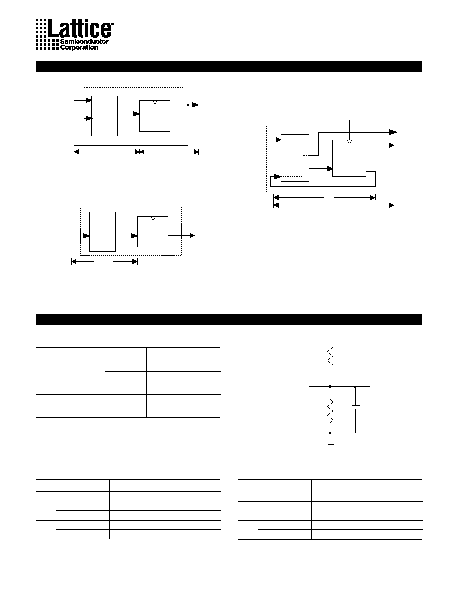
The following discussion pertains to configuring the output logic
macrocell. It should be noted that actual implementation is accom-
plished by development software/hardware and is completely trans-
parent to the user.
There are three global OLMC configuration modes possible:
simple, complex, and registered. Details of each of these modes
is illustrated in the following pages. Two global bits, SYN and AC0,
control the mode configuration for all macrocells. The XOR bit of
each macrocell controls the polarity of the output in any of the three
modes, while the AC1 bit of each of the macrocells controls the in-
put/output configuration. These two global and 16 individual archi-
tecture bits define all possible configurations in a GAL20V8 . The
information given on these architecture bits is only to give a bet-
ter understanding of the device. Compiler software will transpar-
ently set these architecture bits from the pin definitions, so the user
should not need to directly manipulate these architecture bits.
The following is a list of the PAL architectures that the GAL20V8
can emulate. It also shows the OLMC mode under which the
devices emulate the PAL architecture.
Software compilers support the three different global OLMC modes
as different device types. These device types are listed in the table
below. Most compilers have the ability to automatically select the
device type, generally based on the register usage and output
enable (OE) usage. Register usage on the device forces the soft-
ware to choose the registered mode. All combinatorial outputs with
OE controlled by the product term will force the software to choose
the complex mode. The software will choose the simple mode only
when all outputs are dedicated combinatorial without OE control.
The different device types listed in the table can be used to override
the automatic device selection by the software. For further details,
refer to the compiler software manuals.
When using compiler software to configure the device, the user
must pay special attention to the following restrictions in each mode.
In registered mode pin 1 and pin 13 (DIP pinout) are permanently
configured as clock and output enable, respectively. These pins
cannot be configured as dedicated inputs in the registered mode.
In complex mode pin 1 and pin 13 become dedicated inputs and
use the feedback paths of pin 22 and pin 15 respectively. Because
of this feedback path usage, pin 22 and pin 15 do not have the
feedback option in this mode.
In simple mode all feedback paths of the output pins are routed
via the adjacent pins. In doing so, the two inner most pins ( pins
18 and 19) will not have the feedback option as these pins are
always configured as dedicated combinatorial output.
Registered
Complex
Simple
Auto Mode Select
ABEL
P20V8R
P20V8C
P20V8AS
P20V8
CUPL
G20V8MS
G20V8MA
G20V8AS
G20V8
LOG/iC
GAL20V8_R
GAL20V8_C7
GAL20V8_C8
GAL20V8
OrCAD-PLD
"Registered"
1
"Complex"
1
"Simple"
1
GAL20V8A
PLDesigner
P20V8R
2
P20V8C
2
P20V8C
2
P20V8A
TANGO-PLD
G20V8R
G20V8C
G20V8AS
3
G20V8
1) Used with Configuration keyword.
2) Prior to Version 2.0 support.
3) Supported on Version 1.20 or later.
PAL Architectures
GAL20V8
Emulated by GAL20V8
Global OLMC Mode
20R8
Registered
20R6
Registered
20R4
Registered
20RP8
Registered
20RP6
Registered
20RP4
Registered
20L8
Complex
20H8
Complex
20P8
Complex
14L8
Simple
16L6
Simple
18L4
Simple
20L2
Simple
14H8
Simple
16H6
Simple
18H4
Simple
20H2
Simple
14P8
Simple
16P6
Simple
18P4
Simple
20P2
Simple
Output Logic Macrocell (OLMC)
Compiler Support for OLMC

4
Specifications
GAL20V8
In the Registered mode, macrocells are configured as dedicated
registered outputs or as I/O functions.
Architecture configurations available in this mode are similar to the
common 20R8 and 20RP4 devices with various permutations of
polarity, I/O and register placement.
All registered macrocells share common clock and output enable
control pins. Any macrocell can be configured as registered or I/
O. Up to eight registers or up to eight I/Os are possible in this mode.
Dedicated input or output functions can be implemented as sub-
sets of the I/O function.
Registered outputs have eight product terms per output. I/Os have
seven product terms per output.
The JEDEC fuse numbers, including the User Electronic Signature
(UES) fuses and the Product Term Disable (PTD) fuses, are shown
on the logic diagram on the following page.
Registered Configuration for Registered Mode
- SYN=0.
- AC0=1.
- XOR=0 defines Active Low Output.
- XOR=1 defines Active High Output.
- AC1=0 defines this output configuration.
- Pin 1 controls common CLK for the registered outputs.
- Pin 13 controls common
OE
for the registered outputs.
- Pin 1 & Pin 13 are permanently configured as CLK &
OE
for registered output configuration.
Combinatorial Configuration for Registered Mode
- SYN=0.
- AC0=1.
- XOR=0 defines Active Low Output.
- XOR=1 defines Active High Output.
- AC1=1 defines this output configuration.
- Pin 1 & Pin 13 are permanently configured as CLK &
OE
for registered output configuration..
Note: The development software configures all of the architecture control bits and checks for proper pin usage automatically.
D
Q
Q
CLK
OE
XOR
XOR
Registered Mode

Specifications
GAL20V8
5
DIP (PLCC) Package Pinouts
OE
0000
PTD
2640
0280
0320
0600
0640
0920
0960
1240
1280
1560
1600
1880
1920
2200
2240
2520
OLMC
OLMC
XOR-2567
AC1-2639
OLMC
XOR-2566
AC1-2638
OLMC
XOR-2565
AC1-2637
OLMC
XOR-2564
AC1-2636
XOR-2563
AC1-2635
OLMC
XOR-2562
AC1-2634
OLMC
OLMC
XOR-2561
AC1-2633
XOR-2560
AC1-2632
11(13)
10(12)
9(11)
8(10)
7(9)
6(7)
5(6)
4(5)
3(4)
2(3)
1(2)
23(27)
22(26)
21(25)
20(24)
19(23)
18(21)
17(20)
16(19)
15(18)
14(17)
13(16)
SYN-2704
AC0-2705
2703
28
24
36
32
20
16
12
8
4
0
Registered Mode Logic Diagram

6
Specifications
GAL20V8
In the Complex mode, macrocells are configured as output only or
I/O functions.
Architecture configurations available in this mode are similar to the
common 20L8 and 20P8 devices with programmable polarity in
each macrocell.
Up to six I/Os are possible in this mode. Dedicated inputs or outputs
can be implemented as subsets of the I/O function. The two outer
most macrocells (pins 15 & 22) do not have input capability. De-
signs requiring eight I/Os can be implemented in the Registered
mode.
All macrocells have seven product terms per output. One product
term is used for programmable output enable control. Pins 1 and
13 are always available as data inputs into the AND array.
The JEDEC fuse numbers including the UES fuses and PTD fuses
are shown on the logic diagram on the following page.
Note: The development software configures all of the architecture control bits and checks for proper pin usage automatically.
Combinatorial I/O Configuration for Complex Mode
- SYN=1.
- AC0=1.
- XOR=0 defines Active Low Output.
- XOR=1 defines Active High Output.
- AC1=1.
- Pin 16 through Pin 21 are configured to this function.
Combinatorial Output Configuration for Complex Mode
- SYN=1.
- AC0=1.
- XOR=0 defines Active Low Output.
- XOR=1 defines Active High Output.
- AC1=1.
- Pin 15 and Pin 22 are configured to this function.
XOR
XOR
Complex Mode

Specifications
GAL20V8
7
DIP (PLCC) Package Pinouts
0000
PTD
2640
0280
0320
0600
0640
0920
0960
1240
1280
1560
1600
1880
1920
2200
2240
2520
SYN-2704
AC0-2705
OLMC
OLMC
OLMC
OLMC
OLMC
OLMC
OLMC
OLMC
23(27)
22(26)
21(25)
20(24)
19(23)
18(21)
17(20)
16(19)
15(18)
14(17)
13(16)
11(13)
10(12)
9(11)
8(10)
7(9)
6(7)
5(6)
4(5)
3(4)
2(3)
1(2)
2703
XOR-2567
AC1-2639
XOR-2566
AC1-2638
XOR-2565
AC1-2637
XOR-2564
AC1-2636
XOR-2563
AC1-2635
XOR-2562
AC1-2634
XOR-2561
AC1-2633
XOR-2560
AC1-2632
28
24
36
32
20
16
12
8
4
0
Complex Mode Logic Diagram

8
Specifications
GAL20V8
Combinatorial Output with Feedback Configuration
for Simple Mode
- SYN=1.
- AC0=0.
- XOR=0 defines Active Low Output.
- XOR=1 defines Active High Output.
- AC1=0 defines this configuration.
- All OLMC except pins 18 & 19 can be configured to
this function.
Combinatorial Output Configuration for Simple Mode
- SYN=1.
- AC0=0.
- XOR=0 defines Active Low Output.
- XOR=1 defines Active High Output.
- AC1=0 defines this configuration.
- Pins 18 & 19 are permanently configured to this
function.
Dedicated Input Configuration for Simple Mode
- SYN=1.
- AC0=0.
- XOR=0 defines Active Low Output.
- XOR=1 defines Active High Output.
- AC1=1 defines this configuration.
- All OLMC except pins 18 & 19 can be configured to
this function.
Note: The development software configures all of the architecture control bits and checks for proper pin usage automatically.
In the Simple mode, pins are configured as dedicated inputs or as
dedicated, always active, combinatorial outputs.
Architecture configurations available in this mode are similar to the
common 14L8 and 16P6 devices with many permutations of ge-
neric output polarity or input choices.
All outputs in the simple mode have a maximum of eight product
terms that can control the logic. In addition, each output has pro-
grammable polarity.
Pins 1 and 13 are always available as data inputs into the AND
array. The "center" two macrocells (pins 18 and 19) cannot be used
in the input configuration.
The JEDEC fuse numbers including the UES fuses and PTD fuses
are shown on the logic diagram on the following page.
Vcc
XOR
Vcc
XOR
Simple Mode
Specifications
GAL20V8
9
DIP (PLCC) Package Pinouts
0000
PTD
2640
0280
0320
0600
0640
0920
0960
1240
1280
1560
1600
1880
1920
2200
2240
2520
OLMC
OLMC
OLMC
OLMC
OLMC
OLMC
OLMC
XOR-2560
AC1-2632
OLMC
XOR-2561
AC1-2633
XOR-2562
AC1-2634
XOR-2563
AC1-2635
XOR-2564
AC1-2636
XOR-2565
AC1-2637
XOR-2566
AC1-2638
XOR-2567
AC1-2639
23(27)
22(26)
21(25)
20(24)
19(23)
18(21)
17(20)
16(19)
15(18)
14(17)
13(16)
SYN-2704
AC0-2705
2703
11(13)
10(12)
9(11)
8(10)
7(9)
6(7)
5(6)
4(5)
3(4)
2(3)
1(2)
28
24
36
32
20
16
12
8
4
0
Simple Mode Logic Diagram

10
Specifications
GAL20V8
Specifications
GAL20V8C
V
IL
Input Low Voltage
Vss � 0.5
--
0.8
V
V
IH
Input High Voltage
2.0
--
Vcc+1
V
I
IL
1
Input or I/O Low Leakage Current
0V
V
IN
V
IL
(MAX.)
--
--
�100
�
A
I
IH
Input or I/O High Leakage Current
3.5V
V
IN
V
CC
--
--
10
�
A
V
OL
Output Low Voltage
I
OL
= MAX. Vin = V
IL
or V
IH
--
--
0.5
V
V
OH
Output High Voltage
I
OH
= MAX. Vin = V
IL
or V
IH
2.4
--
--
V
I
OL
Low Level Output Current
--
--
16
mA
I
OH
High Level Output Current
--
--
�3.2
mA
I
OS
2
Output Short Circuit Current
V
CC
= 5V
V
OUT
= 0.5V
T
A
= 25
�
C
�30
--
�150
mA
Recommended Operating Conditions
Commercial Devices:
Ambient Temperature (T
A
) ............................... 0 to 75
�
C
Supply voltage (V
CC
)
with Respect to Ground ..................... +4.75 to +5.25V
Industrial Devices:
Ambient Temperature (T
A
) ........................... �40 to 85
�
C
Supply voltage (V
CC
)
with Respect to Ground ..................... +4.50 to +5.50V
SYMBOL
PARAMETER
CONDITION
MIN.
TYP.
3
MAX.
UNITS
COMMERCIAL
I
CC
Operating Power
V
IL
= 0.5V V
IH
= 3.0V
L -5/-7/-10
--
75
115
mA
Supply Current
f
toggle
= 15MHz Outputs Open
INDUSTRIAL
I
CC
Operating Power
V
IL
= 0.5V V
IH
= 3.0V
L-10
--
75
130
mA
Supply Current
f
toggle
= 15MHz Outputs Open
1) The leakage current is due to the internal pull-up resistor on all pins. See Input Buffer section for more information.
2) One output at a time for a maximum duration of one second. Vout = 0.5V was selected to avoid test problems caused by tester
ground degradation. Characterized but not 100% tested.
3) Typical values are at Vcc = 5V and T
A
= 25
�
C
Absolute Maximum Ratings
(1)
Supply voltage V
CC
...................................... �0.5 to +7V
Input voltage applied .......................... �2.5 to V
CC
+1.0V
Off-state output voltage applied ......... �2.5 to V
CC
+1.0V
Storage Temperature ................................ �65 to 150
�
C
Ambient Temperature with
Power Applied ........................................ �55 to 125
�
C
1.Stresses above those listed under the "Absolute Maximum
Ratings" may cause permanent damage to the device. These
are stress only ratings and functional operation of the device at
these or at any other conditions above those indicated in the
operational sections of this specification is not implied (while
programming, follow the programming specifications).
DC Electrical Characteristics
Over Recommended Operating Conditions (Unless Otherwise Specified)

Specifications
GAL20V8
11
Specifications
GAL20V8C
-7
MIN. MAX.
-10
MIN. MAX.
t
pd
A
Input or I/O to
8 outputs switching
1
5
3
7.5
3
10
ns
Comb. Output
1 output switching
--
--
--
7
--
--
ns
t
co
A
Clock to Output Delay
1
4
2
5
2
7
ns
t
cf
2
--
Clock to Feedback Delay
--
3
--
3
--
6
ns
t
su
--
Setup Time, Input or Feedback before Clock
3
--
5
--
7.5
--
ns
t
h
--
Hold Time, Input or Feedback after Clock
0
--
0
--
0
--
ns
A
Maximum Clock Frequency with
142.8 --
100
--
66.7
--
MHz
External Feedback, 1/(tsu + tco)
f
max
3
A
Maximum Clock Frequency with
166
--
125
--
71.4
--
MHz
Internal Feedback, 1/(tsu + tcf)
A
Maximum Clock Frequency with
166
--
125
--
83.3
--
MHz
No Feedback
t
wh
--
Clock Pulse Duration, High
3
--
4
--
6
--
ns
t
wl
--
Clock Pulse Duration, Low
3
--
4
--
6
--
ns
t
en
B
Input or I/O to Output Enabled
1
6
3
9
3
10
ns
B
OE to Output Enabled
1
6
2
6
2
10
ns
t
dis
C
Input or I/O to Output Disabled
1
5
2
9
2
10
ns
C
OE to Output Disabled
1
5
1.5
6
1.5
10
ns
UNITS
PARAMETER
TEST
COND
1
.
DESCRIPTION
COM/IND
COM
COM
-5
MIN. MAX.
1) Refer to Switching Test Conditions section.
2) Calculated from fmax with internal feedback. Refer to fmax Descriptions section.
3) Refer to fmax Descriptions section. Characterized initially and after any design or process changes that may affect these
parameters.
SYMBOL
PARAMETER
MAXIMUM*
UNITS
TEST CONDITIONS
C
I
Input Capacitance
8
pF
V
CC
= 5.0V, V
I
= 2.0V
C
I/O
I/O Capacitance
8
pF
V
CC
= 5.0V, V
I/O
= 2.0V
*Characterized but not 100% tested
AC Switching Characteristics
Over Recommended Operating Conditions
Capacitance (T
A
= 25
�
C, f = 1.0 MHz)
12
Specifications
GAL20V8
Specifications
GAL20V8B
INDUSTRIAL
I
CC
Operating Power
V
IL
= 0.5V V
IH
= 3.0V
L -10/-15/-25
--
75
130
mA
Supply Current
f
toggle
= 15MHz Outputs Open
Q -20/-25
--
45
65
mA
COMMERCIAL
I
CC
Operating Power
V
IL
= 0.5V V
IH
= 3.0V
L -7/-10
--
75
115
mA
Supply Current
f
toggle
= 15MHz Outputs Open
L -15/-25
--
75
90
mA
Q -15/-25
--
45
55
mA
Recommended Operating Conditions
Commercial Devices:
Ambient Temperature (T
A
) ............................... 0 to 75
�
C
Supply voltage (V
CC
)
with Respect to Ground ..................... +4.75 to +5.25V
Industrial Devices:
Ambient Temperature (T
A
) ........................... �40 to 85
�
C
Supply voltage (V
CC
)
with Respect to Ground ..................... +4.50 to +5.50V
DC Electrical Characteristics
Over Recommended Operating Conditions (Unless Otherwise Specified)
SYMBOL
PARAMETER
CONDITION
MIN.
TYP.
3
MAX.
UNITS
V
IL
Input Low Voltage
Vss � 0.5
--
0.8
V
V
IH
Input High Voltage
2.0
--
Vcc+1
V
I
IL
1
Input or I/O Low Leakage Current
0V
V
IN
V
IL
(MAX.)
--
--
�
100
�
A
I
IH
Input or I/O High Leakage Current
3.5V
V
IN
V
CC
--
--
10
�
A
V
OL
Output Low Voltage
I
OL
= MAX. Vin = V
IL
or V
IH
--
--
0.5
V
V
OH
Output High Voltage
I
OH
= MAX. Vin = V
IL
or V
IH
2.4
--
--
V
I
OL
Low Level Output Current
--
--
24
mA
I
OH
High Level Output Current
--
--
�3.2
mA
I
OS
2
Output Short Circuit Current
V
CC
= 5V
V
OUT
= 0.5V
T
A
= 25
�
C
�30
--
�150
mA
1) The leakage current is due to the internal pull-up resistor on all pins. See Input Buffer section for more information.
2) One output at a time for a maximum duration of one second. Vout = 0.5V was selected to avoid test problems caused by tester
ground degradation. Characterized but not 100% tested.
3) Typical values are at Vcc = 5V and T
A
= 25
�
C
Absolute Maximum Ratings
(1)
Supply voltage V
CC
...................................... �0.5 to +7V
Input voltage applied .......................... �2.5 to V
CC
+1.0V
Off-state output voltage applied ......... �2.5 to V
CC
+1.0V
Storage Temperature ................................ �65 to 150
�
C
Ambient Temperature with
Power Applied ........................................ �55 to 125
�
C
1.Stresses above those listed under the "Absolute Maximum
Ratings" may cause permanent damage to the device. These
are stress only ratings and functional operation of the device at
these or at any other conditions above those indicated in the
operational sections of this specification is not implied (while
programming, follow the programming specifications).

Specifications
GAL20V8
13
Specifications
GAL20V8B
t
pd
A
Input or I/O to
8 outputs switching
3
7.5
3
10
3
15
3
20
3
25
ns
Comb. Output
1 output switching
--
7
--
--
--
--
--
--
--
--
ns
t
co
A
Clock to Output Delay
2
5
2
7
2
10
2
11
2
12
ns
t
cf
2
--
Clock to Feedback Delay
--
3
--
6
--
8
--
9
--
10
ns
t
su
--
Setup Time, Input or Fdbk before Clk
7
--
10
--
12
--
13
--
15
--
ns
t
h
--
Hold Time, Input or Fdbk after Clk
0
--
0
--
0
--
0
--
0
--
ns
A
Maximum Clock Frequency with
83.3
--
58.8
--
45.5
--
41.6
--
37
--
MHz
External Feedback, 1/(tsu + tco)
f
max
3
A
Maximum Clock Frequency with
100
--
62.5
--
50
--
45.4
--
40
--
MHz
Internal Feedback, 1/(tsu + tcf)
A
Maximum Clock Frequency with
100
--
62.5
--
62.5
--
50
--
41.7
--
MHz
No Feedback
t
wh
--
Clock Pulse Duration, High
5
--
8
--
8
--
10
--
12
--
ns
t
wl
--
Clock Pulse Duration, Low
5
--
8
--
8
--
10
--
12
--
ns
t
en
B
Input or I/O to Output Enabled
3
9
3
10
--
15
--
18
--
25
ns
B
OE to Output Enabled
2
6
2
10
--
15
--
18
--
20
ns
t
dis
C
Input or I/O to Output Disabled
2
9
2
10
--
15
--
18
--
25
ns
C
OE to Output Disabled
1.5
6
1.5
10
--
15
--
18
--
20
ns
UNITS
1) Refer to Switching Test Conditions section.
2) Calculated from fmax with internal feedback. Refer to fmax Descriptions section.
3) Refer to fmax Descriptions section.
-25
MIN.
MAX.
-20
MIN.
MAX.
-15
MIN.
MAX.
-10
MIN.
MAX.
PARAM.
DESCRIPTION
TEST
COND
1
.
-7
MIN.
MAX.
SYMBOL
PARAMETER
MAXIMUM*
UNITS
TEST CONDITIONS
C
I
Input Capacitance
8
pF
V
CC
= 5.0V, V
I
= 2.0V
C
I/O
I/O Capacitance
8
pF
V
CC
= 5.0V, V
I/O
= 2.0V
*Characterized but not 100% tested.
COM
COM / IND
COM / IND
IND
COM / IND
AC Switching Characteristics
Over Recommended Operating Conditions
Capacitance (TA = 25
�
C, f = 1.0 MHz)
14
Specifications
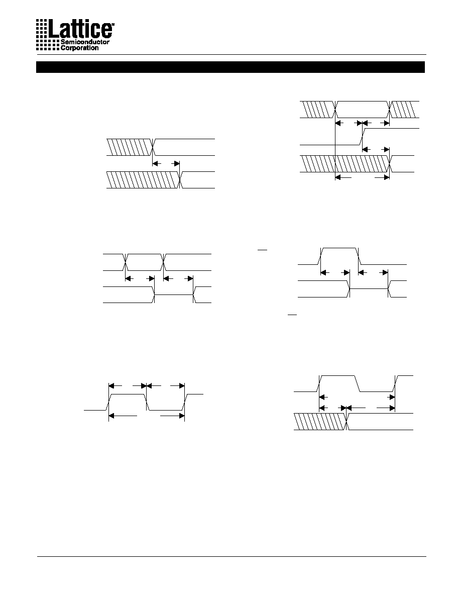
GAL20V8
Registered Output
Combinatorial Output
OE to Output Enable/Disable
Input or I/O to Output Enable/Disable
f
max with Feedback
Clock Width
COMBINATIONAL
OUTPUT
VALID INPUT
INPUT or
I/O FEEDBACK
t
pd
CLK
(w/o fb)
1/
f
max
t
wl
t
wh
INPUT or
I/O FEEDBACK
REGISTERED
OUTPUT
CLK
VALID INPUT
(external fdbk)
t
su
t
co
t
h
1/
f
max
OE
REGISTERED
OUTPUT
t
en
t
dis
CLK
REGISTERED
FEEDBACK
t
cf
t
su
1/
f
max (internal fdbk)
COMBINATIONAL
OUTPUT
INPUT or
I/O FEEDBACK
t
en
t
dis
Switching Waveforms
Specifications
GAL20V8
15
f
max with Internal Feedback 1/(
t
su+
t
cf)
Note: tcf is a calculated value, derived by subtracting tsu from
the period of fmax w/internal feedback (tcf = 1/fmax - tsu). The
value of tcf is used primarily when calculating the delay from
clocking a register to a combinatorial output (through registered
feedback), as shown above. For example, the timing from clock
to a combinatorial output is equal to tcf + tpd.
f
max with No Feedback
Note: fmax with no feedback may be less than 1/(twh + twl). This
is to allow for a clock duty cycle of other than 50%.
GAL20V8C Output Load Conditions (see figure)
Test Condition
R
1
R
2
C
L
A
200
200
50pF
B
Active High
200
50pF
Active Low
200
200
50pF
C
Active High
200
5pF
Active Low
200
200
5pF
TEST POINT
C *
L
FROM OUTPUT (O/Q)
UNDER TEST
+5V
*C
L
INCLUDES TEST FIXTURE AND PROBE CAPACITANCE
R
2
R
1
GAL20V8B Output Load Conditions (see figure)
Test Condition
R
1
R
2
C
L
A
200
390
50pF
B
Active High
390
50pF
Active Low
200
390
50pF
C
Active High
390
5pF
Active Low
200
390
5pF
CLK
REGISTER
LOGIC
ARRAY
t
cf
t
pd
f
max with External Feedback 1/(
t
su+
t
co)
Note: fmax with external feedback is calculated from measured
tsu and tco.
R E G I S T E R
L O G I C
A R R A Y
t
c o
t
s u
C L K
Input Pulse Levels
GND to 3.0V
Input Rise and
GAL20V8B
2 � 3ns 10% � 90%
Fall Times
GAL20V8C
1.5ns 10% � 90%
Input Timing Reference Levels
1.5V
Output Timing Reference Levels
1.5V
Output Load
See Figure
3-state levels are measured 0.5V from steady-state active
level.
REGISTER
LOGIC
ARRAY
CLK
t
su +
t
h
f
max Descriptions
Switching Test Conditions
16
Specifications
GAL20V8
1 . 0
2 . 0
3 . 0
4 . 0
5 . 0
- 6 0
0
- 2 0
- 4 0
0
In p u t V o lt ag e ( V o lt s)
I
nput
C
u
r
r
e
nt
(
u
A
)
Electronic Signature
An electronic signature is provided in every GAL20V8 device. It
contains 64 bits of reprogrammable memory that can contain user
defined data. Some uses include user ID codes, revision numbers,
or inventory control. The signature data is always available to the
user independent of the state of the security cell.
NOTE: The electronic signature is included in checksum calcula-
tions. Changing the electronic signature will alter the checksum.
Security Cell
A security cell is provided in the GAL20V8 devices to prevent un-
authorized copying of the array patterns. Once programmed, this
cell prevents further read access to the functional bits in the device.
This cell can only be erased by re-programming the device, so the
original configuration can never be examined once this cell is pro-
grammed. The Electronic Signature is always available to the user,
regardless of the state of this control cell.
Latch-Up Protection
GAL20V8 devices are designed with an on-board charge pump
to negatively bias the substrate. The negative bias minimizes the
potential of latch-up caused by negative input undershoots. Ad-
ditionally, outputs are designed with n-channel pull-ups instead of
the traditional p-channel pull-ups in order to eliminate latch-up due
to output overshoots.
Device Programming
GAL devices are programmed using a Lattice Semiconductor-
approved Logic Programmer, available from a number of manu-
facturers. Complete programming of the device takes only a few
seconds. Erasing of the device is transparent to the user, and is
done automatically as part of the programming cycle.
Typical Input Pull-up Characteristic
Output Register Preload
When testing state machine designs, all possible states and state
transitions must be verified in the design, not just those required
in the normal machine operations. This is because, in system
operation, certain events occur that may throw the logic into an
illegal state (power-up, line voltage glitches, brown-outs, etc.). To
test a design for proper treatment of these conditions, a way must
be provided to break the feedback paths, and force any desired (i.e.,
illegal) state into the registers. Then the machine can be sequenced
and the outputs tested for correct next state conditions.
GAL20V8 devices include circuitry that allows each registered
output to be synchronously set either high or low. Thus, any present
state condition can be forced for test sequencing. If necessary,
approved GAL programmers capable of executing text vectors
perform output register preload automatically.
Input Buffers
GAL20V8 devices are designed with TTL level compatible input
buffers. These buffers have a characteristically high impedance,
and present a much lighter load to the driving logic than bipolar TTL
devices.
The GAL20V8 input and I/O pins have built-in active pull-ups. As
a result, unused inputs and I/O's will float to a TTL "high" (logical
"1"). Lattice Semiconductor recommends that all unused inputs
and tri-stated I/O pins be connected to another active input, V
CC
,
or Ground. Doing this will tend to improve noise immunity and re-
duce I
CC
for the device.

Specifications
GAL20V8
17
Typ. Vref = 3.2V
Typical Output
Typ. Vref = 3.2V
Typical Input
Vcc
PIN
Vcc
Vref
Active Pull-up
Circuit
ESD
Protection
Circuit
ESD
Protection
Circuit
Vcc
PIN
Vcc
PIN
Vref
Tri-State
Control
Active Pull-up
Circuit
Feedback
(To Input Buffer)
PIN
Feedback
Data
Output
Circuitry within the GAL20V8 provides a reset signal to all registers
during power-up. All internal registers will have their Q outputs set
low after a specified time (
t
pr, 1
�
s MAX). As a result, the state on
the registered output pins (if they are enabled) will always be high
on power-up, regardless of the programmed polarity of the output
pins. This feature can greatly simplify state machine design by pro-
viding a known state on power-up. Because of the asynchronous
nature of system power-up, some conditions must be met to provide
Vcc
CLK
INTERNAL REGISTER
Q - OUTPUT
FEEDBACK/EXTERNAL
OUTPUT REGISTER
Vcc (min.)
t
pr
Internal Register
Reset to Logic "0"
Device Pin
Reset to Logic "1"
t
wl
t
su
a valid power-up reset of the device. First, the V
CC
rise must be
monotonic. Second, the clock input must be at static TTL level as
shown in the diagram during power up. The registers will reset
within a maximum of
t
pr time. As in normal system operation, avoid
clocking the device until all input and feedback path setup times
have been met. The clock must also meet the minimum pulse width
requirements.
Power-Up Reset
Input/Output Equivalent Schematics

18
Specifications
GAL20V8
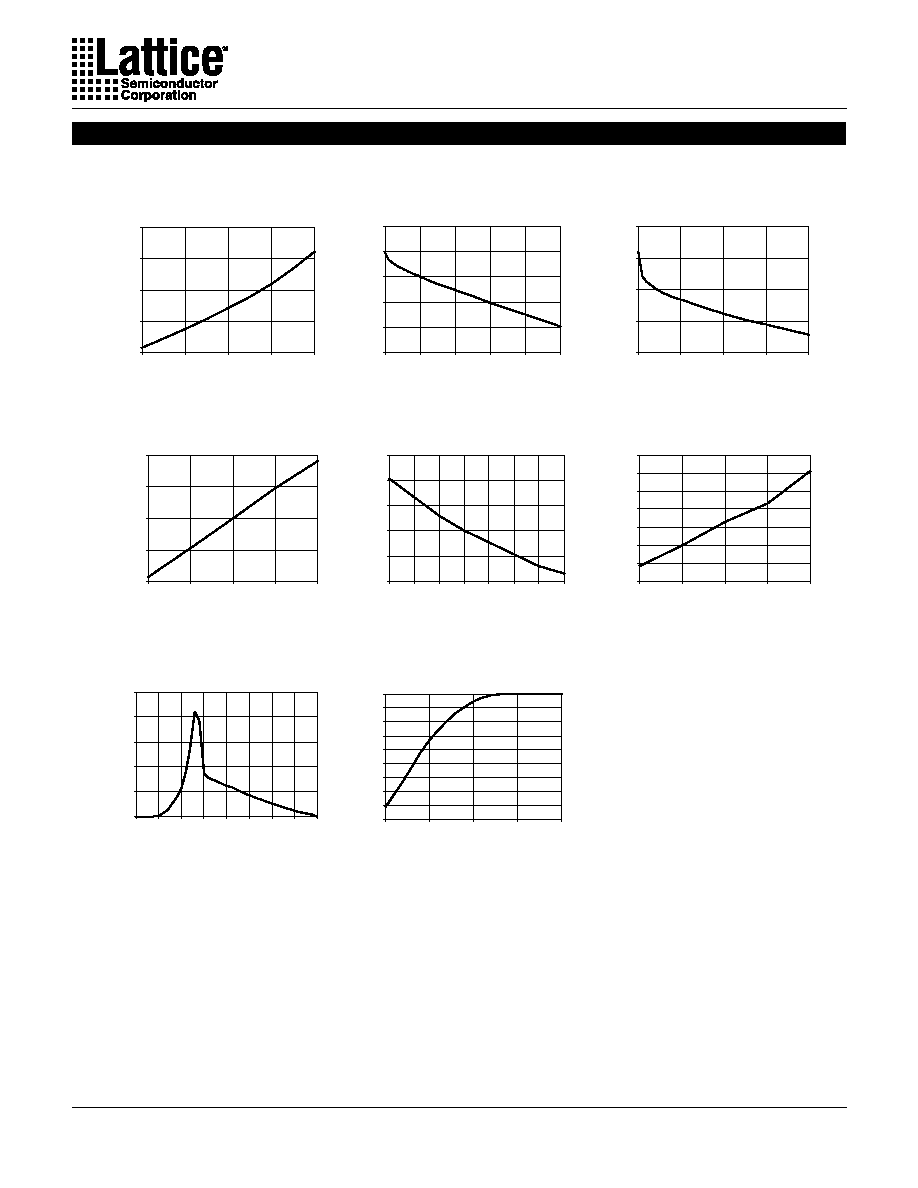
Delta Tpd vs # of Outputs
Switching
Number of Outputs Switching
Delta Tpd (ns)
-1
-0.75
-0.5
-0.25
0
1
2
3
4
5
6
7
8
RISE
FALL
Delta Tco vs # of Outputs
Switching
Number of Outputs Switching
Delta Tco (ns)
-1
-0.75
-0.5
-0.25
0
1
2
3
4
5
6
7
8
RISE
FALL
Delta Tpd vs Output Loading
Output Loading (pF)
Delta Tpd (ns)
-2
0
2
4
6
8
0
50
100
150
200
250
300
RISE
FALL
Delta Tco vs Output Loading
Output Loading (pF)
Delta Tco (ns)
-2
0
2
4
6
8
0
50
100
150
200
250
300
RISE
FALL
Normalized Tpd vs Vcc
Supply Voltage (V)
Normalized Tpd
0.8
0.9
1
1.1
1.2
4.50
4.75
5.00
5.25
5.50
PT H->L
PT L->H
Normalized Tco vs Vcc
Supply Voltage (V)
Normalized Tco
0.8
0.9
1
1.1
1.2
4.50
4.75
5.00
5.25
5.50
RISE
FALL
Normalized Tsu vs Vcc
Supply Voltage (V)
Normalized Tsu
0.8
0.9
1
1.1
1.2
4.50
4.75
5.00
5.25
5.50
PT H->L
PT L->H
Normalized Tpd vs Temp
Temperature (deg. C)
Normalized Tpd
0.7
0.8
0.9
1
1.1
1.2
1.3
-55
-25
0
25
50
75
100
125
PT H->L
PT L->H
Normalized Tco vs Temp
Temperature (deg. C)
Normalized Tco
0.7
0.8
0.9
1
1.1
1.2
1.3
-55
-25
0
25
50
75
100
125
RISE
FALL
Normalized Tsu vs Temp
Temperature (deg. C)
Normalized Tsu
0.7
0.8
0.9
1
1.1
1.2
1.3
1.4
-55
-25
0
25
50
75
100
125
PT H->L
PT L->H
GAL20V8C: Typical AC and DC Characteristic Diagrams
Specifications
GAL20V8
19
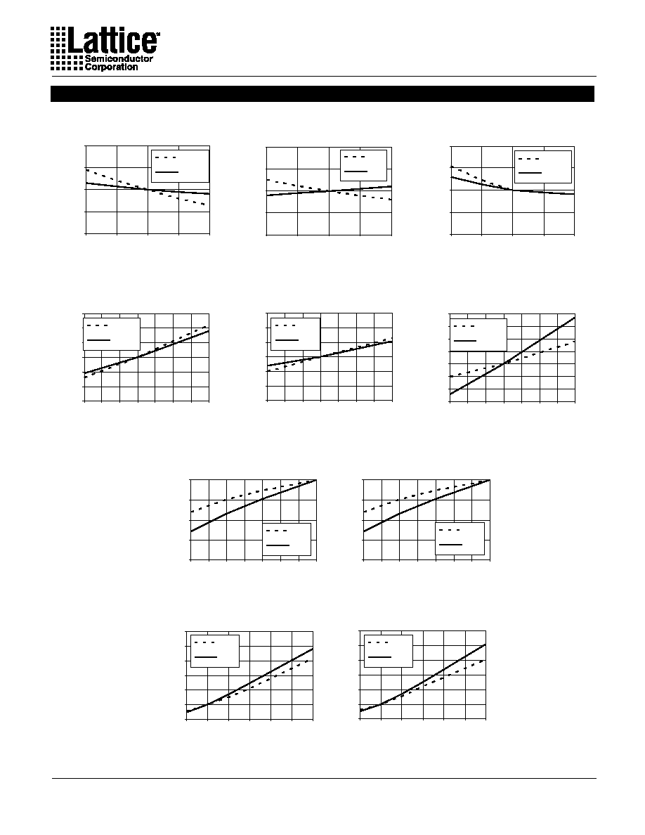
Vol vs Iol
Iol (mA)
Vol (V)
0
0.5
1
1.5
2
0.00
20.00
40.00
60.00
80.00
Voh vs Ioh
Ioh(mA)
Voh (V)
0
1
2
3
4
5
0.00
10.00
20.00
30.00
40.00
50.00
Voh vs Ioh
Ioh(mA)
Voh (V)
3.25
3.5
3.75
4
4.25
0.00
1.00
2.00
3.00
4.00
Normalized Icc vs Vcc
Supply Voltage (V)
Normalized Icc
0.80
0.90
1.00
1.10
1.20
4.50
4.75
5.00
5.25
5.50
Normalized Icc vs Temp
Temperature (deg. C)
Normalized Icc
0.8
0.9
1
1.1
1.2
1.3
-55
-25
0
25
50
75
100
125
Normalized Icc vs Freq.
Frequency (MHz)
Normalized Icc
0.80
0.90
1.00
1.10
1.20
1.30
1.40
1.50
0
25
50
75
100
Delta Icc vs Vin (1 input)
Vin (V)
Delta Icc (mA)
0
2
4
6
8
10
0.00 0.50 1.00 1.50 2.00 2.50 3.00 3.50 4.00
Input Clamp (Vik)
Vik (V)
Iik (mA)
0
5
10
15
20
25
30
35
40
45
-2.00
-1.50
-1.00
-0.50
0.00
GAL20V8C: Typical AC and DC Characteristic Diagrams
20
Specifications
GAL20V8
Normalized Tpd vs Vcc
Supply Voltage (V)
Normalized Tpd
0.8
0.9
1
1.1
1.2
4.50
4.75
5.00
5.25
5.50
PT H->L
PT L->H
Normalized Tco vs Vcc
Supply Voltage (V)
Normalized Tco
0.8
0.9
1
1.1
1.2
4.50
4.75
5.00
5.25
5.50
RISE
FALL
Normalized Tsu vs Vcc
Supply Voltage (V)
Normalized Tsu
0.8
0.9
1
1.1
1.2
4.50
4.75
5.00
5.25
5.50
PT H->L
PT L->H
Normalized Tpd vs Temp
Temperature (deg. C)
Normalized Tpd
0.7
0.8
0.9
1
1.1
1.2
1.3
-55
-25
0
25
50
75
100
125
PT H->L
PT L->H
Normalized Tco vs Temp
Temperature (deg. C)
Normalized Tco
0.7
0.8
0.9
1
1.1
1.2
1.3
-55
-25
0
25
50
75
100
125
RISE
FALL
Normalized Tsu vs Temp
Temperature (deg. C)
Normalized Tsu
0.7
0.8
0.9
1
1.1
1.2
1.3
1.4
-55
-25
0
25
50
75
100
125
PT H->L
PT L->H
Delta Tpd vs # of Outputs
Switching
Number of Outputs Switching
Delta Tpd (ns)
-2
-1.5
-1
-0.5
0
1
2
3
4
5
6
7
8
RISE
FALL
Delta Tco vs # of Outputs
Switching
Number of Outputs Switching
Delta Tco (ns)
-2
-1.5
-1
-0.5
0
1
2
3
4
5
6
7
8
RISE
FALL
Delta Tpd vs Output Loading
Output Loading (pF)
Delta Tpd (ns)
-2
0
2
4
6
8
10
0
50
100
150
200
250
300
RISE
FALL
Delta Tco vs Output Loading
Output Loading (pF)
Delta Tco (ns)
-2
0
2
4
6
8
10
0
50
100
150
200
250
300
RISE
FALL
GAL20V8B-7/-10: Typical AC and DC Characteristic Diagrams

Specifications
GAL20V8
21
Vol vs Iol
Iol (mA)
Vol (V)
0
0.25
0.5
0.75
1
0.00
20.00
40.00
60.00
80.00
100.00
Voh vs Ioh
Ioh(mA)
Voh (V)
0
1
2
3
4
5
0.00
10.00
20.00
30.00
40.00
50.00
60.00
Voh vs Ioh
Ioh(mA)
Voh (V)
3.5
3.75
4
4.25
4.5
0.00
1.00
2.00
3.00
4.00
Normalized Icc vs Vcc
Supply Voltage (V)
Normalized Icc
0.80
0.90
1.00
1.10
1.20
4.50
4.75
5.00
5.25
5.50
Normalized Icc vs Temp
Temperature (deg. C)
Normalized Icc
0.8
0.9
1
1.1
1.2
-55
-25
0
25
50
75
100
125
Normalized Icc vs Freq.
Frequency (MHz)
Normalized Icc
0.80
0.90
1.00
1.10
1.20
1.30
0
25
50
75
100
Delta Icc vs Vin (1 input)
Vin (V)
Delta Icc (mA)
0
2
4
6
8
10
0.00 0.50 1.00 1.50 2.00 2.50 3.00 3.50 4.00
Input Clamp (Vik)
Vik (V)
Iik (mA)
0
10
20
30
40
50
60
70
80
90
100
-2.00
-1.50
-1.00
-0.50
0.00
GAL20V8B-7/-10: Typical AC and DC Characteristic Diagrams

22
Specifications
GAL20V8
Normalized Tpd vs Vcc
Supply Voltage (V)
Normalized Tpd
0.8
0.9
1
1.1
1.2
4.50
4.75
5.00
5.25
5.50
PT H->L
PT L->H
Normalized Tco vs Vcc
Supply Voltage (V)
Normalized Tco
0.8
0.9
1
1.1
1.2
4.50
4.75
5.00
5.25
5.50
RISE
FALL
Normalized Tsu vs Vcc
Supply Voltage (V)
Normalized Tsu
0.8
0.9
1
1.1
1.2
4.50
4.75
5.00
5.25
5.50
PT H->L
PT L->H
Normalized Tpd vs Temp
Temperature (deg. C)
Normalized Tpd
0.7
0.8
0.9
1
1.1
1.2
1.3
-55
-25
0
25
50
75
100
125
PT H->L
PT L->H
Normalized Tco vs Temp
Temperature (deg. C)
Normalized Tco
0.7
0.8
0.9
1
1.1
1.2
1.3
-55
-25
0
25
50
75
100
125
RISE
FALL
Normalized Tsu vs Temp
Temperature (deg. C)
Normalized Tsu
0.7
0.8
0.9
1
1.1
1.2
1.3
1.4
-55
-25
0
25
50
75
100
125
PT H->L
PT L->H
Delta Tpd vs # of Outputs
Switching
Number of Outputs Switching
Delta Tpd (ns)
-2
-1.5
-1
-0.5
0
1
2
3
4
5
6
7
8
RISE
FALL
Delta Tco vs # of Outputs
Switching
Number of Outputs Switching
Delta Tco (ns)
-2
-1.5
-1
-0.5
0
1
2
3
4
5
6
7
8
RISE
FALL
Delta Tpd vs Output Loading
Output Loading (pF)
Delta Tpd (ns)
-4
-2
0
2
4
6
8
10
0
50
100
150
200
250
300
RISE
FALL
Delta Tco vs Output Loading
Output Loading (pF)
Delta Tco (ns)
-4
-2
0
2
4
6
8
10
0
50
100
150
200
250
300
RISE
FALL
GAL20V8B-15/-25: Typical AC and DC Characteristic Diagrams
Specifications
GAL20V8
23
Vol vs Iol
Iol (mA)
Vol (V)
0
0.5
1
1.5
2
0.00
20.00
40.00
60.00
80.00
100.00
Voh vs Ioh
Ioh(mA)
Voh (V)
0
1
2
3
4
5
0.00
10.00
20.00
30.00
40.00
50.00
60.00
Voh vs Ioh
Ioh(mA)
Voh (V)
3.25
3.5
3.75
4
4.25
0.00
1.00
2.00
3.00
4.00
Normalized Icc vs Vcc
Supply Voltage (V)
Normalized Icc
0.80
0.90
1.00
1.10
1.20
4.50
4.75
5.00
5.25
5.50
Normalized Icc vs Temp
Temperature (deg. C)
Normalized Icc
0.8
0.9
1
1.1
1.2
-55
-25
0
25
50
75
100
125
Normalized Icc vs Freq.
Frequency (MHz)
Normalized Icc
0.80
0.90
1.00
1.10
1.20
1.30
1.40
0
25
50
75
100
Delta Icc vs Vin (1 input)
Vin (V)
Delta Icc (mA)
0
2
4
6
8
10
12
0.00 0.50 1.00 1.50 2.00 2.50 3.00 3.50 4.00
Input Clamp (Vik)
Vik (V)
Iik (mA)
0
10
20
30
40
50
60
70
80
90
100
-2.00
-1.50
-1.00
-0.50
0.00
GAL20V8B-15/-25: Typical AC and DC Characteristic Diagrams