GAL20V8
High Performance E
2
CMOS PLD
Generic Array LogicTM
1
2
28
NC
I/CLK
I
I
I
I
I
I
I
NC
NC
NC
GND
I
I
I/OE
I
I/O/Q
I/O/Q
I/O/Q
I/O/Q
I/O/Q
I/O/Q
I/O/Q
Vcc
I/O/Q
I
I
4
5
7
9
11
12
14
16
18
19
21
23
25
26
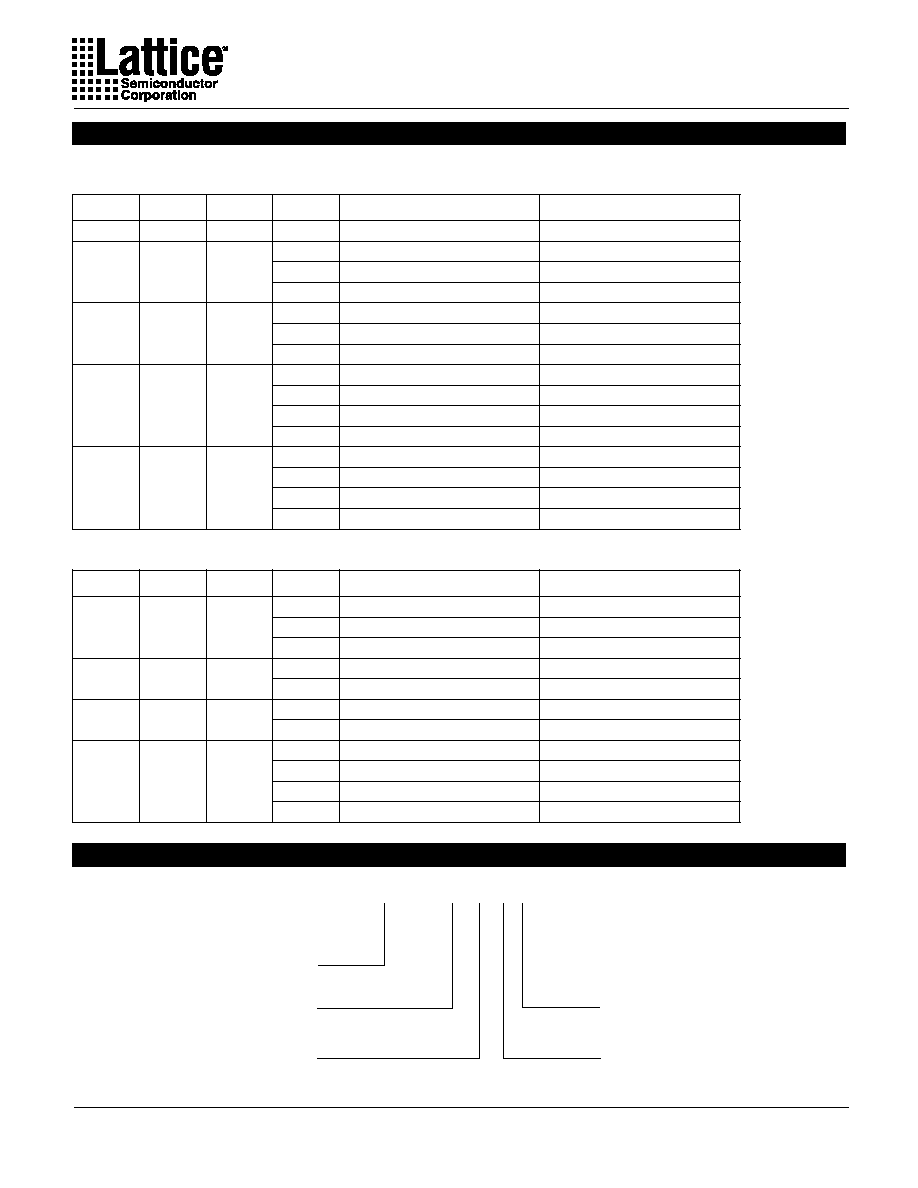
PLCC
1
12
13
24
I/CLK
I
I
I
I
I
I
I
I
I
I
GND
Vcc
I
I/O/Q
I/O/Q
I/O/Q
I/O/Q
I/O/Q
I/O/Q
I/O/Q
I/O/Q
I
I/OE
6
18
GAL20V8
Top View
GAL
20V8
DIP
CLK
I
I
I/O/Q
I/O/Q
I/O/Q
I/O/Q
I/O/Q
I/O/Q
I/O/Q
I/O/Q
I
I
I
I
I
I
I
I
I
I
I/OE
I/CLK
OE
8
8
8
8
8
8
8
8
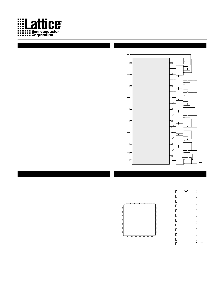
OLMC
OLMC
OLMC
OLMC
OLMC
OLMC
OLMC
IMUX
IMUX
PROGRAMMABLE
AND-ARRAY
(64 X 40)
OLMC
Copyright � 2000 Lattice Semiconductor Corp. All brand or product names are trademarks or registered trademarks of their respective holders. The specifications and information herein are subject
to change without notice.
LATTICE SEMICONDUCTOR CORP., 5555 Northeast Moore Ct., Hillsboro, Oregon 97124, U.S.A.
August 2000
Tel. (503) 268-8000; 1-800-LATTICE; FAX (503) 268-8556; http://www.latticesemi.com
20v8_04
Features
� HIGH PERFORMANCE E
2
CMOS
�
TECHNOLOGY
-- 5 ns Maximum Propagation Delay
-- Fmax = 166 MHz
-- 4 ns Maximum from Clock Input to Data Output
-- UltraMOS
�
Advanced CMOS Technology
� 50% to 75% REDUCTION IN POWER FROM BIPOLAR
-- 75mA Typ Icc on Low Power Device
-- 45mA Typ Icc on Quarter Power Device
� ACTIVE PULL-UPS ON ALL PINS
� E
2
CELL TECHNOLOGY
-- Reconfigurable Logic
-- Reprogrammable Cells
-- 100% Tested/100% Yields
-- High Speed Electrical Erasure (<100ms)
-- 20 Year Data Retention
� EIGHT OUTPUT LOGIC MACROCELLS
-- Maximum Flexibility for Complex Logic Designs
-- Programmable Output Polarity
-- Also Emulates 24-pin PAL
�
Devices with Full Function/
Fuse Map/Parametric Compatibility
� PRELOAD AND POWER-ON RESET OF ALL REGISTERS
-- 100% Functional Testability
� APPLICATIONS INCLUDE:
-- DMA Control
-- State Machine Control
-- High Speed Graphics Processing
-- Standard Logic Speed Upgrade
� ELECTRONIC SIGNATURE FOR IDENTIFICATION
Description
The GAL20V8C, at 5ns maximum propagation delay time, com-
bines a high performance CMOS process with Electrically Eras-
able (E
2
) floating gate technology to provide the highest speed
performance available in the PLD market. High speed erase times
(<100ms) allow the devices to be reprogrammed quickly and ef-
ficiently.
The generic architecture provides maximum design flexibility by
allowing the Output Logic Macrocell (OLMC) to be configured by
the user. An important subset of the many architecture configura-
tions possible with the GAL20V8 are the PAL
architectures listed
in the table of the macrocell description section. GAL20V8 devices
are capable of emulating any of these PAL architectures with full
function/fuse map/parametric compatibility.
Unique test circuitry and reprogrammable cells allow complete AC,
DC, and functional testing during manufacture. As a result, Lattice
Semiconductor delivers 100% field programmability and function-
ality of all GAL products. In addition, 100 erase/write cycles and
data retention in excess of 20 years are specified.
Functional Block Diagram
Pin Configuration
2
Specifications
GAL20V8
)
s
n
(
d
p
T
)
s
n
(
u
s
T
)
s
n
(
o
c
T
)
A
m
(
c
c
I
#
g
n
i
r
e
d
r
O
e
g
a
k
c
a
P
0
1
0
1
7
0
3
1
8
V
0
2
L
A
G
C
I
J
L
0
1
-
C
C
L
P
d
a
e
L
-
8
2
0
3
1
I
P
L
0
1
-
B
8
V
0
2
L
A
G
P
I
D
c
i
t
s
a
l
P
n
i
P
-
4
2
0
3
1
I
J
L
0
1
-
B
8
V
0
2
L
A
G
C
C
L
P
d
a
e
L
-
8
2
5
1
2
1
0
1
0
3
1
I
P
L
5
1
-
B
8
V
0
2
L
A
G
P
I
D
c
i
t
s
a
l
P
n
i
P
-
4
2
0
3
1
I
J
L
5
1
-
B
8
V
0
2
L
A
G
C
C
L
P
d
a
e
L
-
8
2
0
2
3
1
1
1
5
6
I
P
Q
0
2
-
B
8
V
0
2
L
A
G
P
I
D
c
i
t
s
a
l
P
n
i
P
-
4
2
5
6
I
J
Q
0
2
-
B
8
V
0
2
L
A
G
C
C
L
P
d
a
e
L
-
8
2
5
2
5
1
2
1
5
6
I
P
Q
5
2
-
B
8
V
0
2
L
A
G
P
I
D
c
i
t
s
a
l
P
n
i
P
-
4
2
5
6
I
J
Q
5
2
-
B
8
V
0
2
L
A
G
C
C
L
P
d
a
e
L
-
8
2
0
3
1
I
P
L
5
2
-
B
8
V
0
2
L
A
G
P
I
D
c
i
t
s
a
l
P
n
i
P
-
4
2
0
3
1
I
J
L
5
2
-
B
8
V
0
2
L
A
G
C
C
L
P
d
a
e
L
-
8
2
Industrial Grade Specifications
Blank = Commercial
I = Industrial
Grade
Package
Power
L = Low Power
Q = Quarter Power
Speed (ns)
XXXXXXXX
XX
X
X X
Device Name
_
P = Plastic DIP
J = PLCC
GAL20V8C
GAL20V8B
)
s
n
(
d
p
T
)
s
n
(
u
s
T
)
s
n
(
o
c
T
)
A
m
(
c
c
I
#
g
n
i
r
e
d
r
O
e
g
a
k
c
a
P
5
3
4
5
1
1
J
L
5
-
C
8
V
0
2
L
A
G
C
C
L
P
d
a
e
L
-
8
2
5
.
7
7
5
5
1
1
8
V
0
2
L
A
G
C
J
L
7
-
C
C
L
P
d
a
e
L
-
8
2
5
1
1
P
L
7
-
B
8
V
0
2
L
A
G
P
I
D
c
i
t
s
a
l
P
n
i
P
-
4
2
5
1
1
J
L
7
-
B
8
V
0
2
L
A
G
C
C
L
P
d
a
e
L
-
8
2
0
1
0
1
7
5
1
1
8
V
0
2
L
A
G
C
J
L
0
1
-
C
C
L
P
d
a
e
L
-
8
2
5
1
1
P
L
0
1
-
B
8
V
0
2
L
A
G
P
I
D
c
i
t
s
a
l
P
n
i
P
-
4
2
5
1
1
J
L
0
1
-
B
8
V
0
2
L
A
G
C
C
L
P
d
a
e
L
-
8
2
5
1
2
1
0
1
5
5
P
Q
5
1
-
B
8
V
0
2
L
A
G
P
I
D
c
i
t
s
a
l
P
n
i
P
-
4
2
5
5
J
Q
5
1
-
B
8
V
0
2
L
A
G
C
C
L
P
d
a
e
L
-
8
2
0
9
P
L
5
1
-
B
8
V
0
2
L
A
G
P
I
D
c
i
t
s
a
l
P
n
i
P
-
4
2
0
9
J
L
5
1
-
B
8
V
0
2
L
A
G
C
C
L
P
d
a
e
L
-
8
2
5
2
5
1
2
1
5
5
P
Q
5
2
-
B
8
V
0
2
L
A
G
P
I
D
c
i
t
s
a
l
P
n
i
P
-
4
2
5
5
J
Q
5
2
-
B
8
V
0
2
L
A
G
C
C
L
P
d
a
e
L
-
8
2
0
9
P
L
5
2
-
B
8
V
0
2
L
A
G
P
I
D
c
i
t
s
a
l
P
n
i
P
-
4
2
0
9
J
L
5
2
-
B
8
V
0
2
L
A
G
C
C
L
P
d
a
e
L
-
8
2
GAL20V8 Ordering Information
Commercial Grade Specifications
Part Number Description
Specifications
GAL20V8
3
The following discussion pertains to configuring the output logic
macrocell. It should be noted that actual implementation is accom-
plished by development software/hardware and is completely trans-
parent to the user.
There are three global OLMC configuration modes possible:
simple, complex, and registered. Details of each of these modes
is illustrated in the following pages. Two global bits, SYN and AC0,
control the mode configuration for all macrocells. The XOR bit of
each macrocell controls the polarity of the output in any of the three
modes, while the AC1 bit of each of the macrocells controls the in-
put/output configuration. These two global and 16 individual archi-
tecture bits define all possible configurations in a GAL20V8 . The
information given on these architecture bits is only to give a bet-
ter understanding of the device. Compiler software will transpar-
ently set these architecture bits from the pin definitions, so the user
should not need to directly manipulate these architecture bits.
The following is a list of the PAL architectures that the GAL20V8
can emulate. It also shows the OLMC mode under which the
devices emulate the PAL architecture.
Software compilers support the three different global OLMC modes
as different device types. These device types are listed in the table
below. Most compilers have the ability to automatically select the
device type, generally based on the register usage and output
enable (OE) usage. Register usage on the device forces the soft-
ware to choose the registered mode. All combinatorial outputs with
OE controlled by the product term will force the software to choose
the complex mode. The software will choose the simple mode only
when all outputs are dedicated combinatorial without OE control.
The different device types listed in the table can be used to override
the automatic device selection by the software. For further details,
refer to the compiler software manuals.
When using compiler software to configure the device, the user
must pay special attention to the following restrictions in each mode.
In registered mode pin 1 and pin 13 (DIP pinout) are permanently
configured as clock and output enable, respectively. These pins
cannot be configured as dedicated inputs in the registered mode.
In complex mode pin 1 and pin 13 become dedicated inputs and
use the feedback paths of pin 22 and pin 15 respectively. Because
of this feedback path usage, pin 22 and pin 15 do not have the
feedback option in this mode.
In simple mode all feedback paths of the output pins are routed
via the adjacent pins. In doing so, the two inner most pins ( pins
18 and 19) will not have the feedback option as these pins are
always configured as dedicated combinatorial output.
Registered
Complex
Simple
Auto Mode Select
ABEL
P20V8R
P20V8C
P20V8AS
P20V8
CUPL
G20V8MS
G20V8MA
G20V8AS
G20V8
LOG/iC
GAL20V8_R
GAL20V8_C7
GAL20V8_C8
GAL20V8
OrCAD-PLD
"Registered"
1
"Complex"
1
"Simple"
1
GAL20V8A
PLDesigner
P20V8R
2
P20V8C
2
P20V8C
2
P20V8A
TANGO-PLD
G20V8R
G20V8C
G20V8AS
3
G20V8
1) Used with Configuration keyword.
2) Prior to Version 2.0 support.
3) Supported on Version 1.20 or later.
PAL Architectures
GAL20V8
Emulated by GAL20V8
Global OLMC Mode
20R8
Registered
20R6
Registered
20R4
Registered
20RP8
Registered
20RP6
Registered
20RP4
Registered
20L8
Complex
20H8
Complex
20P8
Complex
14L8
Simple
16L6
Simple
18L4
Simple
20L2
Simple
14H8
Simple
16H6
Simple
18H4
Simple
20H2
Simple
14P8
Simple
16P6
Simple
18P4
Simple
20P2
Simple
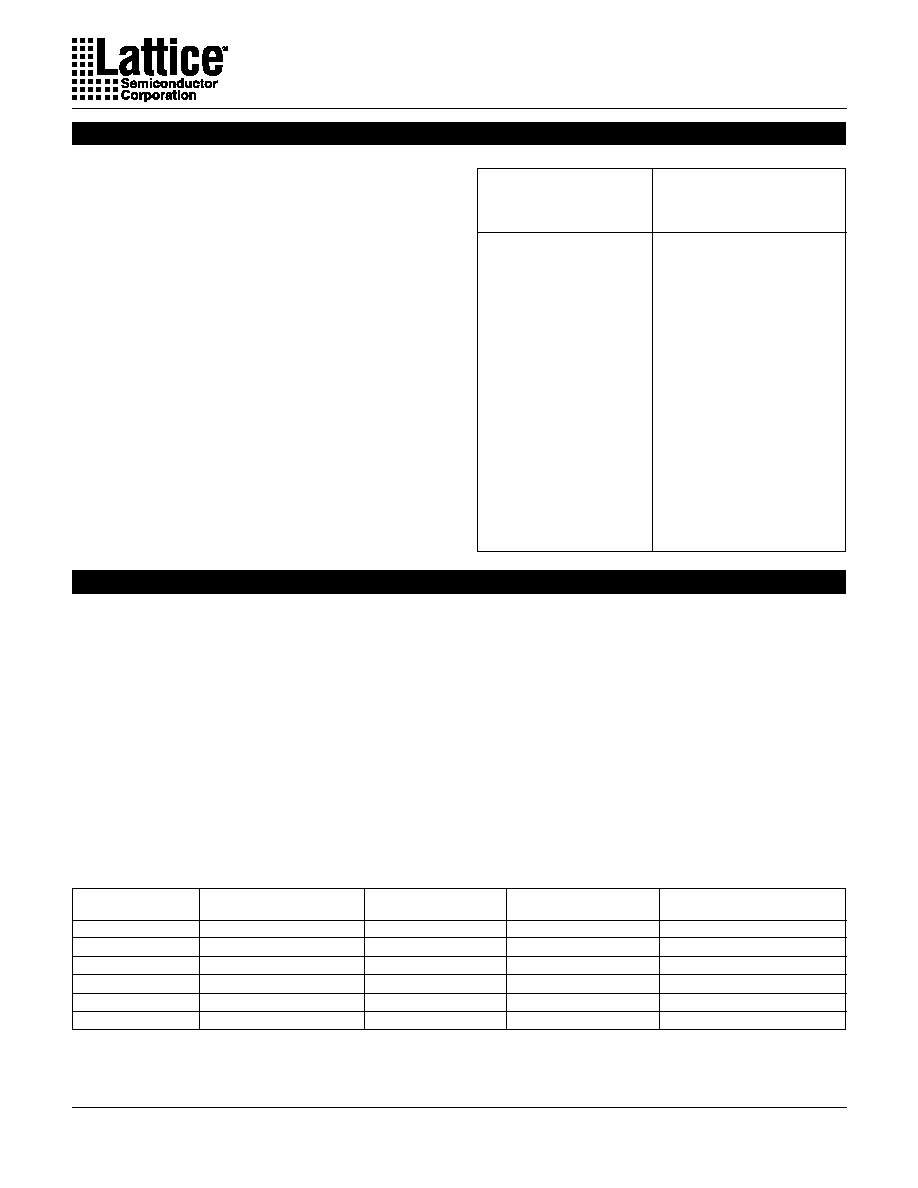
Output Logic Macrocell (OLMC)
Compiler Support for OLMC

4
Specifications
GAL20V8
In the Registered mode, macrocells are configured as dedicated
registered outputs or as I/O functions.
Architecture configurations available in this mode are similar to the
common 20R8 and 20RP4 devices with various permutations of
polarity, I/O and register placement.
All registered macrocells share common clock and output enable
control pins. Any macrocell can be configured as registered or I/
O. Up to eight registers or up to eight I/Os are possible in this mode.
Dedicated input or output functions can be implemented as sub-
sets of the I/O function.
Registered outputs have eight product terms per output. I/Os have
seven product terms per output.
The JEDEC fuse numbers, including the User Electronic Signature
(UES) fuses and the Product Term Disable (PTD) fuses, are shown
on the logic diagram on the following page.
Registered Configuration for Registered Mode
- SYN=0.
- AC0=1.
- XOR=0 defines Active Low Output.
- XOR=1 defines Active High Output.
- AC1=0 defines this output configuration.
- Pin 1 controls common CLK for the registered outputs.
- Pin 13 controls common
OE
for the registered outputs.
- Pin 1 & Pin 13 are permanently configured as CLK &
OE
for registered output configuration.
Combinatorial Configuration for Registered Mode
- SYN=0.
- AC0=1.
- XOR=0 defines Active Low Output.
- XOR=1 defines Active High Output.
- AC1=1 defines this output configuration.
- Pin 1 & Pin 13 are permanently configured as CLK &
OE
for registered output configuration..
Note: The development software configures all of the architecture control bits and checks for proper pin usage automatically.
D
Q
Q
CLK
OE
XOR
XOR
Registered Mode

Specifications
GAL20V8
5
DIP (PLCC) Package Pinouts
OE
0000
PTD
2640
0280
0320
0600
0640
0920
0960
1240
1280
1560
1600
1880
1920
2200
2240
2520
OLMC
OLMC
XOR-2567
AC1-2639
OLMC
XOR-2566
AC1-2638
OLMC
XOR-2565
AC1-2637
OLMC
XOR-2564
AC1-2636
XOR-2563
AC1-2635
OLMC
XOR-2562
AC1-2634
OLMC
OLMC
XOR-2561
AC1-2633
XOR-2560
AC1-2632
11(13)
10(12)
9(11)
8(10)
7(9)
6(7)
5(6)
4(5)
3(4)
2(3)
1(2)
23(27)
22(26)
21(25)
20(24)
19(23)
18(21)
17(20)
16(19)
15(18)
14(17)
13(16)
SYN-2704
AC0-2705
2703
28
24
36
32
20
16
12
8
4
0
Registered Mode Logic Diagram