ispLSI
®
5512VE
In-System Programmable
3.3V SuperWIDETM High Density PLD
1
5512ve_05
Copyright © 2002 Lattice Semiconductor Corp. All brand or product names are trademarks or registered trademarks of their respective holders. The specifications and information herein are subject
to change without notice.
LATTICE SEMICONDUCTOR CORP., 5555 Northeast Moore Ct., Hillsboro, Oregon 97124, U.S.A.
January 2002
Tel. (503) 268-8000; 1-800-LATTICE; FAX (503) 268-8556; http://www.latticesemi.com
Features
· Second Generation SuperWIDE HIGH DENSITY
IN-SYSTEM PROGRAMMABLE LOGIC DEVICE
-- 3.3V Power Supply
-- User Selectable 3.3V/2.5V I/O
-- 24000 PLD Gates / 512 Macrocells
-- Up to 256 I/O Pins
-- 512 Registers
-- High-Speed Global Interconnect
-- SuperWIDE Generic Logic Block (32 Macrocells) for
Optimum Performance
-- SuperWIDE Input Gating (68 Inputs) for Fast
Counters, State Machines, Address Decoders, etc.
-- PCB Efficient Ball Grid Array (BGA) Package Options
-- Interfaces with Standard 5V TTL Devices
· HIGH PERFORMANCE E
2
CMOS
®
TECHNOLOGY
--
f
max = 155 MHz Maximum Operating Frequency
--
t
pd = 6.5 ns Propagation Delay
-- TTL/3.3V/2.5V Compatible Input Thresholds and
Output Levels
-- Electrically Erasable and Reprogrammable
-- Non-Volatile
-- Programmable Speed/Power Logic Path Optimization
· IN-SYSTEM PROGRAMMABLE
-- Increased Manufacturing Yields, Reduced Time-to-
Market, and Improved Product Quality
-- Reprogram Soldered Devices for Faster Debugging
· 100% IEEE 1149.1 BOUNDARY SCAN TESTABLE AND
3.3V IN-SYSTEM PROGRAMMABLE
· ARCHITECTURE FEATURES
-- Enhanced Pin-Locking Architecture with Single-
Level Global Routing Pool and SuperWIDE GLBs
-- Wrap Around Product Term Sharing Array Supports
up to 35 Product Terms Per Macrocell
-- Macrocells Support Concurrent Combinatorial and
Registered Functions
-- Macrocell Registers Feature Multiple Control
Options Including Set, Reset and Clock Enable
-- Four Dedicated Clock Input Pins Plus Macrocell
Product Term Clocks
-- Programmable I/O Supports Programmable Bus
Hold, Pull-up, Open Drain and Slew Rate Options
-- Four Global Product Term Output Enables, Two
Global OE Pins and One Product Term OE per
Macrocell
Global Routing Pool
(GRP)
Boundary
Scan
Interface
Input Bus
Generic
Logic Block
Input Bus
Generic
Logic Block
Input Bus
Input Bus
Input Bus
Input Bus
Generic
Logic Block
Generic
Logic Block
Generic
Logic Block
Generic
Logic Block
Input Bus
Generic
Logic Block
Input Bus
Generic
Logic Block
Input Bus
Generic
Logic Block
Input Bus
Input Bus
Input Bus
Input Bus
Generic
Logic Block
Generic
Logic Block
Generic
Logic Block
Generic
Logic Block
Input Bus
Generic
Logic Block
Input Bus
Generic
Logic Block
Input Bus
Generic
Logic Block
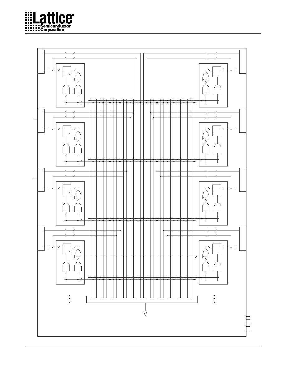
ispLSI 5000VE Description
The ispLSI 5000VE Family of In-System Programmable
High Density Logic Devices is based on Generic Logic
Blocks (GLBs) of 32 registered macrocells and a single
Global Routing Pool (GRP) structure interconnecting the
GLBs.
Outputs from the GLBs drive the Global Routing Pool
(GRP) between the GLBs. Switching resources are pro-
vided to allow signals in the Global Routing Pool to drive
any or all the GLBs in the device. This mechanism allows
fast, efficient connections across the entire device.
Each GLB contains 32 macrocells and a fully populated,
programmable AND-array with 160 logic product terms
and three extra control product terms. The GLB has 68
inputs from the Global Routing Pool which are available
in both true and complement form for every product term.
The 160 product terms are grouped in 32 sets of five and
sent into a Product Term Sharing Array (PTSA) which
allows sharing up to a maximum of 35 product terms for
a single function. Alternatively, the PTSA can be by-
passed for functions of five product terms or less. The
three extra product terms are used for shared controls:
reset, clock, clock enable and output enable.
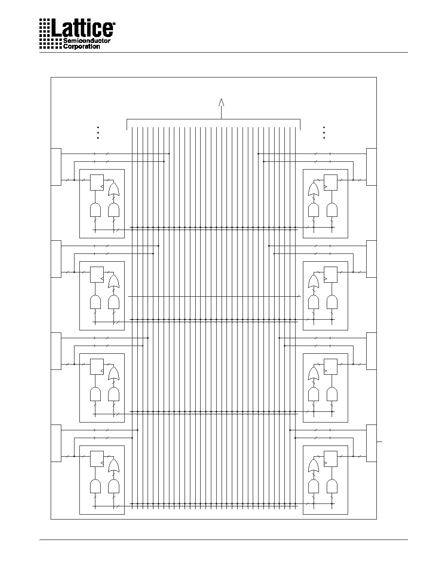
Functional Block Diagram
Specifications
ispLSI 5512VE
2
Functional Block Diagram
Figure 1. ispLSI 5512VE Functional Block Diagram (256-I/O Option)
Package Type
Multiplexed Signals
256 fpBGA
I/O 119 / CLK2 I/O 131 / CLK3
I/O 0 / TOE
272 BGA
I/O 119 / CLK2 I/O 131 / CLK 3
I/O 0 / TOE
388 fpBGA
I/O 179 / CLK2 I/O 197 / CLK 3
I/O 0 / TOE
388 BGA
I/O 179 / CLK2 I/O 197 / CLK 3
I/O 0 / TOE
Global Routing Pool
(GRP)
Boundary
Scan
Interface
GOE0
GOE1
1. CLK2, CLK3 and TOE signals are multiplexed with I/O signals. Use the table below to determine which I/O
is shared by package type.
TDI
TCK
TMS
TDO
CLK 1
CLK 0
1
CLK 3
1
CLK 2
VCCIO
Input Bus
Generic
Logic Block
Input Bus
Generic
Logic Block
Input Bus
Input Bus
Input Bus
Input Bus
Generic
Logic Block
Generic
Logic Block
Generic
Logic Block
Generic
Logic Block
Input Bus
Generic
Logic Block
Input Bus
Generic
Logic Block
Input Bus
Input Bus
Input Bus
Input Bus
Generic
Logic Block
Generic
Logic Block
Generic
Logic Block
Generic
Logic Block
I/O 143
I/O 142
I/O 141
I/O 140
I/O 131
I/O 130
I/O 129
I/O 128
I/O 64
I/O 65
I/O 66
I/O 67
I/O 76
I/O 77
I/O 78
I/O 79
I/O 80
I/O 81
I/O 82
I/O 83
I/O 92
I/O 93
I/O 94
I/O 95
I/O 207
I/O 206
I/O 205
I/O 204
I/O 195
I/O 194
I/O 193
I/O 192
I/O 223
I/O 222
I/O 221
I/O 220
I/O 211
I/O 210
I/O 209
I/O 208
I/O 239
I/O 238
I/O 237
I/O 236
I/O 227
I/O 226
I/O 225
I/O 224
1TOE
I/O 1
I/O 2
I/O 3
I/O 12
I/O 13
I/O 14
I/O 15
I/O 16
I/O 17
I/O 18
I/O 19
I/O 28
I/O 29
I/O 30
I/O 31
I/O 32
I/O 33
I/O 34
I/O 35
I/O 44
I/O 45
I/O 46
I/O 47
Input Bus
Generic
Logic Block
I/O 48
I/O 49
I/O 50
I/O 51
I/O 60
I/O 61
I/O 62
I/O 63
Input Bus
Generic
Logic Block
I/O 108
I/O 109
I/O 110
I/O 111
I/O 96
I/O 97
I/O 98
I/O 99
I/O 124
I/O 125
I/O 126
I/O 127
I/O 112
I/O 113
I/O 114
I/O 115
Input Bus
Generic
Logic Block
I/O 159/CLK2
I/O 158
I/O 157
I/O 156
I/O 147
I/O 146
I/O 145
I/O 144
I/O 175/CLK3
I/O 174
I/O 173
I/O 172
I/O 163
I/O 162
I/O 161
I/O 160
I/O 191
I/O 190
I/O 189
I/O 188
I/O 179
I/O 178
I/O 177
I/O 176
Input Bus
Generic
Logic Block
I/O 255
I/O 254
I/O 253
I/O 252
I/O 243
I/O 242
I/O 241
I/O 240
RESET
Specifications
ispLSI 5512VE
3
ispLSI 5000VE Description (Continued)
The 32 registered macrocells in the GLB are driven by the
32 outputs from the PTSA or the PTSA bypass. Each
macrocell contains a programmable XOR gate, a pro-
grammable register/latch and the necessary clocks and
control logic to allow combinatorial or registered opera-
tion. The macrocells each have two outputs, combinatorial
and registered. This dual output capability from the
macrocell allows efficient use of the hardware resources.
One output can be a registered function for example,
while the other output can be an unrelated combinatorial
function. A direct register input from the I/O pad facili-
tates efficient use of this feature to construct high-speed
input registers.
Macrocell registers can be clocked from one of several
global or product term clocks available on the device. A
global and product term clock enable is also available to
each register, eliminating the need to gate the clock to the
macrocell registers. Reset for the macrocell register is
provided from the global signal, its polarity is user-
selectable. The macrocell register can be programmed to
operate as a D-type register or a D-type latch.
The 32 outputs from the GLB can drive both the Global
Routing Pool and the device I/O cells. The Global Routing
Pool contains one input from each macrocell output and
one input from each I/O pin.
The input buffer threshold has programmable TTL/3.3V/
2.5V compatible levels. The output driver can source
4mA and sink 8mA in 3.3V mode. The output drivers
have a separate VCCIO reference input which is inde-
pendent of the main VCC supply for the device. This
feature allows individual output drivers to drive either
3.3V (from the device VCC) or 2.5V (from the VCCIO pin)
output levels while the device logic and the output current
drive are powered from device supply (VCC). The output
drivers also provide individually programmable edge
rates and open drain capability. A programmable pullup
resistor is provided to tie off unused inputs. Additionally,
a programmable bus-hold latch is available to hold tristate
outputs in their last valid state until the bus is driven again
by some device.
The ispLSI 5000VE Family features 3.3V, non-volatile in-
system programmability for both the logic and the
interconnect structures, providing the means to develop
truly reconfigurable systems. Programming is achieved
through the industry standard IEEE 1149.1-compliant
Boundary Scan interface. Boundary Scan test is also
supported through the same interface.
An enhanced, multiple cell security scheme is provided
that prevents reading of the JEDEC programming file
when secured. After the device has been secured using
this mechanism, the only way to clear the security is to
execute a bulk-erase instruction.
ispLSI 5000VE Family Members
The ispLSI 5000VE Family ranges from 128 macrocells
to 512 macrocells and operates from a 3.3V power
supply. All family members will be available with multiple
package options. The ispLSI 5000VE Family device
matrix showing the various bondout options is shown in
the table below.
The interconnect structure (GRP) is very similar to Lattice's
existing ispLSI 1000, 2000 and 3000 families, but with an
enhanced interconnect structure for optimal pin locking
and logic routing. This eliminates the need for registered
I/O cells or an Output Routing Pool.
The ispLSI 5000VE encompasses the innovative fea-
tures of the ispLSI 5000VA family with several
enhancements. The macrocell is optimized and the T-
type flip flop option is removed. To improve the efficiency
of design fits, the Product Term Reset Logic is simplified
and the polarity option as well as the Global Preset
function are removed. The programmable output-delay
feature (skew option) is also removed. As a result, the
ispLSI 5000VE is not JEDEC compatible with the ispLSI
5000VA. ispLSI 5000VA and 5000VE pinouts may differ
in the same package, however all programming and
power/ground pins are located in the same locations.
Table 1. ispLSI 5000VE Family
Package Type
ispLSI 5128VE
Device
GLBs
Macrocells
128 TQFP
256 fpBGA
272 BGA
388 fpBGA
388 BGA
4
128
96 I/O
--
--
--
--
8
256
96 I/O
144 I/O
144 I/O
--
--
12
384
--
192 I/O
192 I/O
--
--
16
512
--
100 TQFP
--
72 I/O
--
--
192 I/O
192 I/O
256 I/O
256 I/O
ispLSI 5256VE
ispLSI 5384VE
ispLSI 5512VE