Document Outline
- Features
- ispMACH 4000 Introduction
- Overview
- ispMACH 4000 Architecture
- I/O Cell
- Global OE Generation
- Zero Power/Low Power and Power Management
- IEEE 1149.1-Compliant Boundary Scan Testability
- I/O Quick Configuration
- IEEE 1532-Compliant In-System Programming
- Security Bit
- Hot Socketing
- Density Migration
- Absolute Maximum Ratings1, 2, 3
- Recommended Operating Conditions
- Erase Reprogram Specifications
- Hot Socketing Characteristics1,2,3
- I/O Recommended Operating Conditions
- DC Electrical Characteristics
- Supply Current, ispMACH 4000V/B/C�
- Supply Current, ispMACH 4000Z�
- I/O DC Electrical Characteristics
- ispMACH 4000V/B/C External Switching Characteristics
- ispMACH 4000V/B/C External Switching Characteristics (Cont.)
- ispMACH 4032Z External Switching Characteristics1
- Timing Model
- ispMACH 4000V/B/C Internal Timing Parameters�
- ispMACH 4000V/B/C Internal Timing Parameters�
- ispMACH 4032Z Internal Timing Parameters1�
- ispMACH 4000V/B/C Timing Adders1
- ispMACH 4000V/B/C Timing Adders1
- ispMACH 4032Z Timing Adders1, 2
- Boundary Scan Waveforms and Timing Specifications
- Power Consumption
- Power Estimation Coefficients1
- Switching Test Conditions
- Signal Descriptions
- ispMACH 4000V/B/C/Z Power Supply and NC Connections1
- ispMACH 4032V/B/C and 4064V/B/C Logic Signal Connections: 44-Pin TQFP�
- ispMACH 4032V/B/C/Z and 4064V/B/C/Z Logic Signal Connections: 48-Pin TQFP�
- ispMACH 4032Z and 4064Z Logic Signal Connections: 56-Ball csBGA�
- ispMACH 4064V/B/C/Z, 4128V/B/C/Z, 4256V/B/C Logic Signal Connections: 100-Pin TQFP�
- ispMACH 4128V/B/C Logic Signal Connections: 128-Pin TQFP�
- ispMACH 4128V and 4256V Logic Signal Connections: 144-Pin TQFP�
- ispMACH 4256V/B/C, 4384V/B/C, 4512V/B/C, Logic Signal Connections: 176-Pin TQFP�
- ispMACH 4256V/B/C, 4384V/B/C, 4512V/B/C Logic Signal Connections: 256-Ball fpBGA�
- Part Number Description
- Ordering Information
- For Further Information

www.latticesemi.com
1
ispm4k_16z
ispMACH
4000V/B/C/Z Family
3.3V/2.5V/1.8V In-System Programmable
SuperFAST
High Density PLDs
July 2003
Data Sheet
TM
TM
� 2003 Lattice Semiconductor Corp. All Lattice trademarks, registered trademarks, patents, and disclaimers are as listed at www.latticesemi.com/legal. All other brand
or product names are trademarks or registered trademarks of their respective holders. The specifications and information herein are subject to change without notice.
NEW!
Industry's Lo
west
Power CPLDs!
ispMACH 4000
Z
Features
High Performance
� f
MAX
= 400MHz maximum operating frequency
� t
PD
= 2.5ns propagation delay
� Up to four global clock pins with programmable
clock polarity control
� Up to 80 PTs per output
Ease of Design
� Enhanced macrocells with individual clock,
reset, preset and clock enable controls
� Up to four global OE controls
� Individual local OE control per I/O pin
� Excellent First-Time-Fit
TM
and refit
� Fast path, SpeedLocking
TM
Path, and wide-PT
path
� Wide input gating (36 input logic blocks) for fast
counters, state machines and address decoders
Zero Power (ispMACH 4000Z) and Low
Power (ispMACH 4000V/B/C)
� Typical static current 10�A (4032Z)
� Typical static current 1.3mA (4000C)
� 1.8V core low dynamic power
Broad Device Offering
� Multiple temperature range support
� Commercial: 0 to 90�C junction (T
j
)
� Industrial: -40 to 105�C junction (T
j
)
� Automotive: -40 to 130�C junction (T
j
)
Easy System Integration
� Operation with 3.3V, 2.5V or 1.8V LVCMOS I/O
� Operation with 3.3V (4000V), 2.5V (4000B) or
1.8V (4000C/Z) supplies
� 5V tolerant I/O for LVCMOS 3.3, LVTTL, and PCI
interfaces
� Hot-socketing
� Open-drain capability
� Input pull-up, pull-down or bus-keeper
� Programmable output slew rate
� 3.3V PCI compatible
� IEEE 1149.1 boundary scan testable
� 3.3V/2.5V/1.8V In-System Programmable
(ISPTM) using IEEE 1532 compliant interface
� I/O pins with fast setup path
Table 1. ispMACH 4000V/B/C Family Selection Guide
ispMACH
4032V/B/C
ispMACH
4064V/B/C
ispMACH
4128V/B/C
ispMACH
4256V/B/C
ispMACH
4384V/B/C
ispMACH
4512V/B/C
Macrocells
32
64
128
256
384
512
User I/O Options
30/32
30/32/64
64/92/96
64/96/128/160
128/192
128/208
t
PD
(ns)
2.5
2.5
2.7
3.0
3.5
3.5
t
S
(ns)
1.8
1.8
1.8
2.0
2.0
2.0
t
CO
(ns)
2.2
2.2
2.7
2.7
2.7
2.7
f
MAX
(MHz)
400
400
333
322
322
322
Supply Voltages (V)
3.3/2.5/1.8V
3.3/2.5/1.8V
3.3/2.5/1.8V
3.3/2.5/1.8V
3.3/2.5/1.8V
3.3/2.5/1.8V
Pins/Package
44 TQFP
48 TQFP
44 TQFP
48 TQFP
100 TQFP
100 TQFP
128 TQFP
144 TQFP
1
100 TQFP
144 TQFP
1
176 TQFP
256 fpBGA
2
176 TQFP
256 fpBGA
176 TQFP
256 fpBGA
1. 3.3V (4000V) only.
2. 128-I/O and 160-I/O configurations.

Lattice Semiconductor
ispMACH 4000V/B/C/Z Family Data Sheet
2
Table 2. ispMACH 4000Z Family Selection Guide
ispMACH 4000 Introduction
The high performance ispMACH 4000 family from Lattice offers a SuperFAST CPLD solution. The family is a blend
of Lattice's two most popular architectures: the ispLSI
�
2000 and ispMACH 4A. Retaining the best of both families,
the ispMACH 4000 architecture focuses on significant innovations to combine the highest performance with low
power in a flexible CPLD family.
The ispMACH 4000 combines high speed and low power with the flexibility needed for ease of design. With its
robust Global Routing Pool and Output Routing Pool, this family delivers excellent First-Time-Fit, timing predictabil-
ity, routing, pin-out retention and density migration.
The ispMACH 4000 family offers densities ranging from 32 to 512 macrocells. There are multiple density-I/O com-
binations in Thin Quad Flat Pack (TQFP) and Fine Pitch BGA (fpBGA) packages ranging from 44 to 256 pins/balls.
Table 1 shows the macrocell, package and I/O options, along with other key parameters.
The ispMACH 4000 family has enhanced system integration capabilities. It supports 3.3V (4000V), 2.5V (4000B)
and 1.8V (4000C/Z) supply voltages and 3.3V, 2.5V and 1.8V interface voltages. Additionally, inputs can be safely
driven up to 5.5V when an I/O bank is configured for 3.3V operation, making this family 5V tolerant. The ispMACH
4000 also offers enhanced I/O features such as slew rate control, PCI compatibility, bus-keeper latches, pull-up
resistors, pull-down resistors, open drain outputs and hot socketing. The ispMACH 4000 family members are 3.3V/
2.5V/1.8V in-system programmable through the IEEE Standard 1532 interface. IEEE Standard 1149.1 boundary
scan testing capability also allows product testing on automated test equipment.
Overview
The ispMACH 4000 devices consist of multiple 36-input, 16-macrocell Generic Logic Blocks (GLBs) interconnected
by a Global Routing Pool (GRP). Output Routing Pools (ORPs) connect the GLBs to the I/O Blocks (IOBs), which
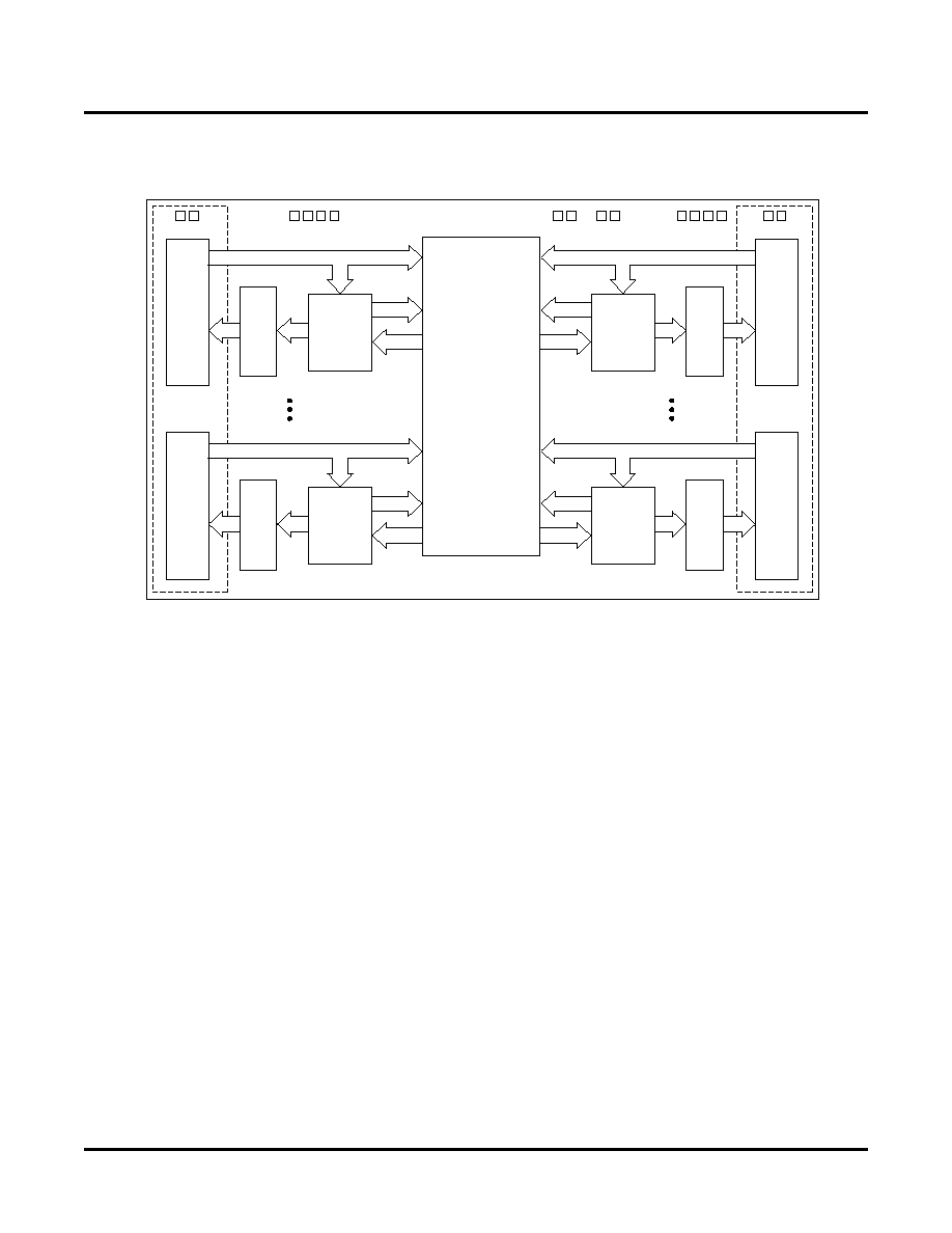
contain multiple I/O cells. This architecture is shown in Figure 1.
ispMACH 4032ZC
1
ispMACH 4064ZC
2
ispMACH 4128ZC
2
ispMACH 4256ZC
2
Macrocells
32
64
128
256
User I/O Options
32
32/64
64/96
64/96/128
t
PD
(ns)
3.5
4.0
4.5
5.0
t
S
(ns)
2.2
2.8
2.9
3.0
t
CO
(ns)
3.0
3.3
3.9
3.9
f
MAX
(MHz)
267
250
220
200
Supply Voltage (V)
1.8
1.8
1.8
1.8
Standby Icc (�A)
20
25
30
40
Pins/Package
48 TQFP
56 csBGA
48 TQFP
56 csBGA
100 TQFP
132 csBGA
100 TQFP
132csBGA
100 TQFP
132 csBGA
176 TQFP
1. Preliminary information.
2. Advance information.
Lattice Semiconductor
ispMACH 4000V/B/C/Z Family Data Sheet
3
Figure 1. Functional Block Diagram
The I/Os in the ispMACH 4000 are split into two banks. Each bank has a separate I/O power supply. Inputs can
support a variety of standards independent of the chip or bank power supply. Outputs support the standards com-
patible with the power supply provided to the bank. Support for a variety of standards helps designers implement
designs in mixed voltage environments. In addition, 5V tolerant inputs are specified within an I/O bank that is con-
nected to V
CCO
of 3.0V to 3.6V for LVCMOS 3.3, LVTTL and PCI interfaces.
ispMACH 4000 Architecture
There are a total of two GLBs in the ispMACH 4032, increasing to 32 GLBs in the ispMACH 4512. Each GLB has
36 inputs. All GLB inputs come from the GRP and all outputs from the GLB are brought back into the GRP to be
connected to the inputs of any other GLB on the device. Even if feedback signals return to the same GLB, they still
must go through the GRP. This mechanism ensures that GLBs communicate with each other with consistent and
predictable delays. The outputs from the GLB are also sent to the ORP. The ORP then sends them to the associ-
ated I/O cells in the I/O block.
Generic Logic Block
The ispMACH 4000 GLB consists of a programmable AND array, logic allocator, 16 macrocells and a GLB clock
generator. Macrocells are decoupled from the product terms through the logic allocator and the I/O pins are decou-
pled from macrocells through the ORP. Figure 2 illustrates the GLB.
I/O
Block
ORP
ORP
16
16
GOE0
GOE1
V
CC
GND
TCK
TMS
TDI
TDO
36
Generic
Logic
Block
Generic
Logic
Block
I/O
Block
ORP
ORP
16
36
Generic
Logic
Block
Generic
Logic
Block
I/O
Block
I/O Bank 0
I/O Bank 1
I/O
Block
36
36
CLK0/I
CLK1/I
CLK2/I
CLK3/I
16
16
Global Routing P
ool
V
CCO0
GND
V
CCO1
GND
16
16
16

Lattice Semiconductor
ispMACH 4000V/B/C/Z Family Data Sheet
4
Figure 2. Generic Logic Block
AND Array
The programmable AND Array consists of 36 inputs and 83 output product terms. The 36 inputs from the GRP are
used to form 72 lines in the AND Array (true and complement of the inputs). Each line in the array can be con-
nected to any of the 83 output product terms via a wired-AND. Each of the 80 logic product terms feed the logic
allocator with the remaining three control product terms feeding the Shared PT Clock, Shared PT Initialization and
Shared PT OE. The Shared PT Clock and Shared PT Initialization signals can optionally be inverted before being
fed to the macrocells.
Every set of five product terms from the 80 logic product terms forms a product term cluster starting with PT0.
There is one product term cluster for every macrocell in the GLB. Figure 3 is a graphical representation of the AND
Array.
Logic Allocator
36 Inputs
from GRP
16 Macrocells
To ORP
To GRP
To
Product Term
Output Enable
Sharing
1+OE
16 MC Feedback Signals
Clock
Generator
1+OE
1+OE
1+OE
1+OE
1+OE
1+OE
CLK0
CLK1
CLK2
CLK3
1+OE
AND Array
36 Inputs,
83 Product Terms

Lattice Semiconductor
ispMACH 4000V/B/C/Z Family Data Sheet
5
Figure 3. AND Array
Enhanced Logic Allocator
Within the logic allocator, product terms are allocated to macrocells in product term clusters. Each product term
cluster is associated with a macrocell. The cluster size for the ispMACH 4000 family is 4+1 (total 5) product terms.
The software automatically considers the availability and distribution of product term clusters as it fits the functions
within a GLB. The logic allocator is designed to provide three speed paths: 5-PT fast bypass path, 20-PT Speed
Locking path and an up to 80-PT path. The availability of these three paths lets designers trade timing variability for
increased performance.
The enhanced Logic Allocator of the ispMACH 4000 family consists of the following blocks:
� Product Term Allocator
� Cluster Allocator
� Wide Steering Logic
Figure 4 shows a macrocell slice of the Logic Allocator. There are 16 such slices in the GLB.
Figure 4. Macrocell Slice
PT0
PT1
Cluster 0
PT2
PT3
PT4
In[0]
In[34]
In[35]
Note:
Indicates programmable fuse.
PT80
PT81
PT82
Shared PT Clock
Shared PT Initialization
Shared PTOE
PT76
PT77
PT78
PT79
PT75
Cluster 15
to
n+1
to
n-1
to
n-2
from
n-1
from
n-4
from
n+2
from
n+1
5-PT
From
n-4
1-80
PTs
To n+4
Fast 5-PT
Path
To XOR (MC)
Cluster
Individual Product
Term Allocator
Cluster
Allocator
SuperWIDETM
Steering Logic
n